0 Preface
The boost type circuits currently used for white light driving mainly include an inductive DC-DC circuit and a charge pump circuit. The inductive DC-DC circuit has problems such as EMI, and the charge pump circuit has a simple structure and a small EMI, and has been widely used.
There are two main types of white light LED driven charge pumps: voltage mode and current mode. Relative to the voltage mode, which may cause the brightness mismatch of each LED, the current mode outputs a constant current separately, so that the brightness can be well matched, and the peripheral balancing resistor is not needed, which greatly saves space.
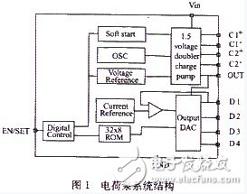
The design of the current-type charge pump circuit for white LED driving proposed in this paper. The design adopts 1.5 times voltage boosting, which improves the efficiency compared with the traditional 2x voltage boost mode, and adopts digital dimming mode to provide 32 gray scale output to meet the requirements of different occasions. The system structure is shown in Figure 1. Mainly can be divided into the following parts: bandgap reference circuit, soft start circuit, oscillator, 1.5 times charge pump, digital dimming module. When the EN/SET terminal inputs a high level, the chip starts, Vin is boosted by 1.5 times the charge pump to stabilize the output voltage at 5 V. If the EN/SET terminal inputs a series of pulses and then sets a high level, the digital dimming The module can record the number of pulses and then convert them into different output currents to achieve the dimming function.
1, 1.5 times the charge pump principle
1.1 Basic principles
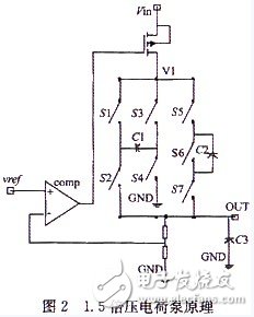
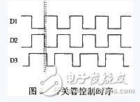
The principle of 1.5 times voltage charge pump is shown in Figure 2. The basic control idea is as follows: OSC controls the conduction and shutdown of S1~S7 through the drive circuit. The timing is as follows: at the first moment, S1, S4, and S6 are turned on, Vin charges capacitor C1, C2 is shorted, VC1=V1, VC2=0; at the second moment, S1, S4, and S6 are turned off, and S2, S3, and S5 are turned on. , S7, C1 charge C2, make VC1=VC2=1/2 V1, and finally add V1 to charge C3, and then cycle again, VCUT is divided by resistor, compare with the reference voltage, control the on-resistance of the upper MOS transistor, change The RC charging constant of the charging circuit finally stabilizes the output at 5 V. Figure 3 shows the timing diagram of the control pulse, where D1 is the driving signal of S1, low effective; D2 is the driving signal of S4, S6, high effective; D3 is S2 The drive signals of S3, S5, and S7 are low effective. In order to prevent clock feedthrough, a non-overlapping clock circuit is included in the driver circuit.
1.2 Actual circuit design
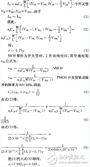
The entire switch network consists of five PMOS transistors S1, S2, S3, S5, S7 and two NMOS transistors S4, S6, as shown in Figure 4. Taking the P pipe S1 and the N pipe S4 as an example, the width to length ratio of the switch pipe is calculated. According to the requirements of the layout design rules, the width/length ratio W/L of a single tube can be set to 2.8 μm/0.6 μm. Suppose the width to length ratio of S1 is x (W/L), and the width to length ratio of S4 is y (W/ L). This design uses CSMC 0.6 μm process, according to process and design requirements, V1=3.3 V, unCOX=50μA/V2 VTHN=0.7 V,|VTHP|=1 V, 2up=un, because
Static Frequency Connerter With Threephase Output
Variable Frequency Inverter,Variable Frequency Converter,3 Phase Frequency Converter,Frequency Converter 60Hz To 50Hz 3 Phase
Jinan Xinyuhua Energy Technology Co.,Ltd , https://www.xyhenergy.com