Introduction to Blood Pressure Monitor
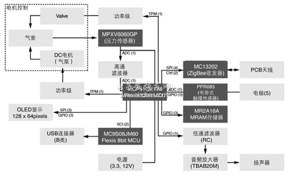
A blood pressure monitor is a device used to measure arterial pressure when blood is pumped away from the heart. Its components include: power supply, motor, memory, pressure sensor and user interface (including display screen, keypad or touchpad, sound device and optional USB or ZigBee communication interface). Figure 1 shows Freescale's blood pressure monitor reference design RDQE128BPM.

Figure 1 Blood pressure monitor reference design RDQE128BPM
How to take a blood pressure measurement
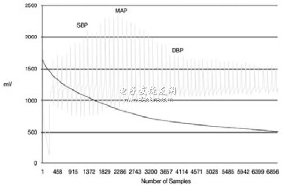
When the cuff surrounding the patient's arm is slowly released, small changes in pressure in the cuff can be noticed. These pressure fluctuations are generated by the patient's heart rhythm cycle, which is then amplified and shifted by a 1 Hz high-pass filter to produce a blood pressure curve. as shown in picture 2. This new signal is the heartbeat signal.
Using the heartbeat detection method described above, a simple oscilloscope method can be used to measure systolic blood pressure (SBP) and diastolic blood pressure (DBP), which is used by most automatic non-invasive blood pressure monitoring devices. When the cuff is inflated above the systolic pressure and then slowly deflated, the magnitude of the pressure change in the cuff is measured. When the pressure is lower than the systolic pressure of blood vessels, this amplitude will suddenly increase. When the pressure in the cuff drops further, the pulse amplitude reaches its maximum value and decreases rapidly. Diastolic blood pressure is obtained at the beginning of this rapid change. Therefore, SBP and DBP are obtained by defining the fast rising region (SBP) and falling region (DBP) of the pulse amplitude. The average arterial blood pressure (MAP) is at its maximum.
Measuring SBP and DBP can help diagnose common hypertension, but clinical monitoring alone cannot distinguish between two common types of hypertension.
Essential hypertension
Primary hypertension is hypertension caused by no clear cause or cause that can be corrected. The judgment of essential hypertension is that the systolic blood pressure is continuously higher than 140mmHg or the diastolic blood pressure is continuously higher than 90mmHg.
White coat hypertension
White coat high blood pressure refers to high blood pressure symptoms that appear only in a highly stressed environment different from the general family environment, such as high blood pressure symptoms caused in a clinic or doctor's office. People with white coat hypertension have high blood pressure readings in the clinic environment, but blood pressure readings return to normal after leaving the clinic. White coat hypertension may be misdiagnosed as essential hypertension, which leads to unnecessary treatment and additional insurance costs. For this reason, medical experts usually recommend a few weeks of measurements at home to determine the diagnosis. Therefore, portable and easy-to-use sphygmomanometers have become popular in homes.
Analog-to-digital conversion accuracy
As shown in Figure 1, the microcontroller (MCU) and pressure sensor are the core technologies of the sphygmomanometer. The RDQE128BPM reference design also illustrates that the most important ADC in this application is the MCU module. The ADC module on the Freescale controller chip is a successive approximation ADC, which includes a sampling latch circuit for obtaining the input voltage, a comparator, a successive approximation register sub-circuit, and an internal reference voltage capacitive DAC.
Blood pressure monitors need to measure very small signals, so ADC resolution is usually a key parameter, such as 10-bit, 12-bit, or 16-bit resolution, which is also an important factor in choosing an MCU for application design. Also important is the accuracy of the ADC. All ADCs have their inherent inaccuracy because they digitize the signal through discrete steps (quantization). Therefore, the digital output cannot perfectly reflect the analog input signal. For example, a 12-bit converter will provide a 1.22mV least significant bit (LSB) for an input voltage of up to 5V. Therefore, the ADC can only digitize the value to a multiple of 1.22mV. In this example, it shows that the best measurement can never be more accurate than the ± 0.5 least significant bit LSB (± 610µV).
Unfortunately, some other embedded ADC features introduce errors and reduce their accuracy. These features include offset, temperature drift, and nonlinearity. 16-bit ADCs used in some ADCs such as Flexis products have the ability to reduce offset and gain errors through calibration. The on-chip temperature sensor on the ADC channel enables temperature compensation to be embodied.
The effective bit of the ADC (ENOB) is a true indicator of resolution and accuracy. This value indicates how many bits in a particular system provide accurate information. It can be calculated by the following formula:
ENOB = (SNR-1.76dB) /6.02dB
Here, SNR (Signal to Noise Ratio) is the ratio between meaningful information (signal) and background noise (noise or error). The signal-to-noise ratio value is not only affected by ADC design and chip integration, but also by printed circuit board (PCB) design, wiring, and selected additional discrete components. A large signal-to-noise ratio value means that more signals are data and the error is small, which can improve the accuracy of the measurement results when measuring signals with microvolt levels.
Improve accuracy
Adding a small amount of controlled "jitter" noise signal (such as 0.5 LSB Gaussian white noise) to the input of the ADC can affect the signal to move up and down the bit closest to the minimum resolution. This method can avoid rounding. The state of the least significant bit of the conversion is randomly jittered between 0 and 1, instead of being fixed at a value. By introducing tiny noise, the extensible ADC can convert the effective range of the signal instead of simply removing all signals at this low level. Again, this introduces quantization errors over the entire range. Dithering only increases resolution and improves linearity, but it does not improve accuracy. However, the accuracy can be improved by adding 1 to 2 bits of least significant bit noise to the signal and using oversampling techniques.
Oversampling is the process of acquiring signals through a sampling rate that is significantly higher than the Nyquist sampling frequency. In fact, oversampling is used to obtain high-resolution ADC converters. For example, a 12-bit converter running at 256 times the target sample rate can be used for 16-bit conversion. For each additional resolution bit, the signal must be oversampled 4 times. Because real-world ADCs cannot perform uninterrupted conversions, the input value should remain constant during the conversion.
The sample and hold circuit accomplishes such a task by this method: a capacitor is used to store the analog voltage at the input, and an electronic switch is used to disconnect the capacitor from the input. Using an ADC that is set to best suit the sampling and holding time of the input signal is very helpful to improve the accuracy of the conversion result.
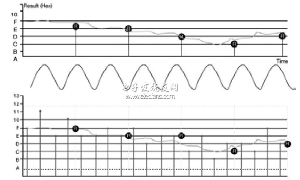
Combining noise coupling and oversampling can further improve accuracy. As shown in Figure 3. This technique is usually considered as oversampling and decimation filtering. The top graph shows the results of the ADC converter over time, and shows what would happen if oversampling alone was used without additional noise. By adding 1 to 2 LSB noises, as indicated by the vertical line at the bottom, simultaneous sampling will not have the same result. This method increases the signal-to-noise ratio and improves the effective bit. By adding 1 ~ 2 LSB noise and oversampling at the input signal, the results can be averaged to provide a more accurate value. The average data obtained from ADC measurements flattens glitches in the input signal, which has the advantage of reducing signal fluctuations and noise.
There are also four sources of error that can be managed: offset, gain, leakage current, and a smaller range of temperature. Some embedded MCU on-chip ADC modules, such as the 16-bit ADC on the new Flexis product, have hardware calibration features that can be calibrated repeatedly during code execution. Embedded ADC modules without hardware calibration can still be calibrated, but this must be done in the factory, or there is a solution designed for the product.

Figure 2 Blood pressure changes in blood pressure measurement

Figure 3 Noise coupling and oversampling combine to further improve accuracy
Calibration is a three-step process: the first step configures the ADC, the second step starts the calibration conversion and waits for the conversion to complete, and finally performs offset and gain calibration.
The offset and gain calibration values ​​can be reduced or amplified depending on the result. This can be done in software or in some implemented ADC hardware.
The input offset is the easiest of the three sources to compensate. For the conversion of a single-ended input, the input can refer to the same internal voltage. This should produce a zero result. If the result is not zero, this is the offset value, which must be subtracted from the ADC result. If the differential conversion mode is used, the offset value can be found by changing the same signal on both input pins.
Once the offset value is known, the gain of the ADC can be found from the full-scale error. This is the difference between the ideal output value at the maximum range (such as 0xFFF in a 12-bit ADC) and the actual output value when the offset value is zero.

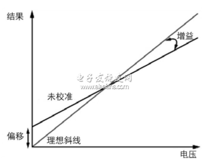
Figure 4 Offset of uncalibrated range and corresponding ideal range
Figure 4 shows the effect of an uncalibrated slope from ground to full scale corresponding to the ideal slope's offset and gain being exaggerated. Depending on the accurate ADC results in the application, in blood pressure monitors, it is required to indicate small changes in readings (µV) and calibration should be performed frequently, at least after each restart. If a hardware function is not present, calibration can be obtained by designing ground and VDD input to the application section, subtracting the offset after each conversion and multiplying by the calculated gain.
There is also a source of input error, that is, the leakage current on the input pin will cause a voltage drop on the input resistance of the input terminal. This error can be tens of times the least significant bit in these battery voltage and temperature detection circuits. The best way to eliminate this error is to reduce the analog DC source resistance and any form of leakage under the control of the designer.
The temperature of the MCU chip can also have an effect on the ADC result. However, temperature is a slowly changing factor. The routine repeated calibration of a blood pressure monitor is designed into the application code, which eliminates the need for the user to consider ideal conditions and minimizes the effect of temperature. However, a complete calibration at the factory (whose results are stored in a look-up table in memory) can basically eliminate the effects of temperature. Many ADCs have on-chip temperature sensors, which can be used to monitor the temperature and make adjustments possible.
Non-linearity is almost a factor that cannot be calibrated because it is usually inherent in module design. The voltage difference between each transcoding should be equal to 1LSB. Therefore, nonlinearity refers to the irregular interval of the coding step, which causes some signal distortion.
Conclusion
Freescale's embedded controller ADC has highly integrated functions, allowing designers to obtain highly accurate measurements. The 16-bit ADC in the latest Flexis product family enables developers to improve accuracy by adjusting the offset and gain of the ADC without increasing the system hardware and software requirements.
Air Core Inductor Coil,Ferrite Core Coil,Winding Air Core Inductors,Copper Induction Coil
IHUA INDUSTRIES CO.,LTD. , https://www.ihua-coil.com