For the first high-performance microcontroller based on the ARM® Cortex®-M7 core in the micro-processing world, the STM32F7 series is believed to be familiar to many people. For example, the STM32F7 series of microcontrollers use a 90nm process and operate at up to 216MHz. They use a 6-stage superscalar pipeline and floating point unit. The test score is up to 1000 CoreMarks. The performance is improved while maintaining high energy efficiency, and the STM32F4 series pins are highly compatible.

In general, ARM® Cortex®-M7 core-based microcontrollers mostly have similar processor configuration options. Usually includes:
- A 64-bit AXI system bus interface
- an instruction and data cache
-64-bit instruction tightly coupled memory (ITCM)
- Dual 32-bit data tightly coupled memory (DTCM)
However, this article only introduces several features of the STM32F7 series from other MCUs that use the Cortex-M7 core from the perspective of application development.
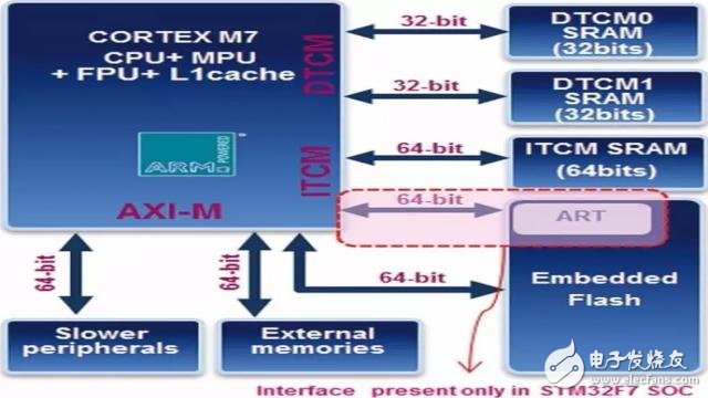
First, the first important feature is that the STM32F7 device has both an ITCM interface and an AXI interface connected to the on-chip flash memory , as shown in Figure 1.

Figure 1: Block diagram of a system-on-chip based on the ARMCortex-M7 core
The presence of the ITCM and AXI dual interfaces gives you more flexibility in executing your code. In addition, the STM32F7 has a built-in flash accelerator called the Adaptive Real-Time Accelerator (ARTAcceleratorTM) for zero-waiting execution of the flash. Similar performance to a cached AXI interface can be achieved using the TCM interface and the ART accelerator. At the same time, the user code does not have the trouble of cache invalidation or cache maintenance operations.
With the ART Accelerator acceleration engine and L1 cache up to 16kB, the STM32F7MCU delivers the best performance of the ARM Cortex-M7. Whether executing code from on-chip flash or external memory, the 1082 CoreMark/462 DMIPS can be achieved at 216MHz.
The second major feature is the internal SRAM distributed in different modules to reduce dynamic power consumption and allow simultaneous access to different SRAM modules from various bus masters to optimize bandwidth and latency.
A typical application example of this architecture is the human-machine interface. In the human-machine interface, the transmission between audio and graphics data and system RAM must be performed simultaneously.
The third is its advanced floating point unit. The STM32F7 family of devices features a high performance single or double precision floating point unit (FPU) that supports all ARM single or dual data processing instructions and data types. FPU offers advantages in many applications that require floating-point math accuracy, including loop control, audio processing, audio decoding, and digital filtering.
It also has the added advantage of allowing the execution or processing of certain functions to be offloaded from the CPU to the FPU, allowing the CPU to be used for other tasks. It supports double precision, making it easier to use PC-based math software for double-precision floating-point instructions.
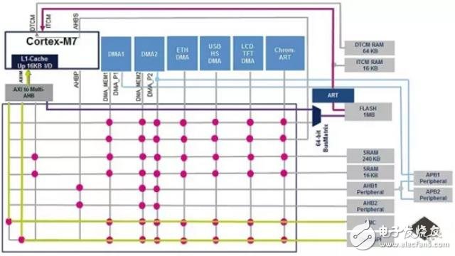
Fourth, one of the most distinctive designs of STM32F7 MCUs is their intelligent system architecture, which uses two subsystems, as shown in Figure 2:

Figure 2: Bus Matrix of the STM32F7 Microcontroller
AXI-to-mulTI-AHB bridge converts AXI4 protocol into AHB-Lite protocol mulTI-AHB bus matrix management host access arbitration This arbitration uses a round-robin scheduling algorithm to ensure host access to the slave, even if multiple high-speed peripherals are simultaneously Work can also achieve simultaneous access and efficient operation.
Finally, I have to mention its L1 cache. The STM32F7 embeds instruction and data caches to compensate for insertion waits when reading code and data from on-chip or off-chip memory, improving performance. Of course, if there is a cache failure and a cache line fill, viewing the cache at this time will not guarantee the certainty of the data.
That's why it's highly recommended to use TCM memory to execute critical code and store critical data. This is often useful in applications where safe operation is required, such as appliances and motors.
Because the cache can be accessed not only by the CPU, but also by other hosts (including direct memory access (DMA) controllers), software maintenance operations are required. When accessing physical storage, these hosts may read out-of-date data, and the updated data is already available in the CPU cache.
To avoid this problem, developers should take the following actions when writing user code:
A. Cache clearing is recommended before a host other than the CPU will perform access to the cache. This is to ensure that the latest update data for the CPU is written back to physical memory.
B. When a host other than the CPU updates the cache data, the CPU should invalidate the cache before reading the cache. This is to ensure direct reading from physical memory.
C. Sometimes there is no need to consider cache operations. When the cache is frequently accessed by other hosts, the CPU can configure non-cacheable attributes to prevent data inconsistency.
Genki Ippai 1.0 uses high-tech temperature control, food grade pod and high-quality material device. We also upgrade to type-C interface for charging faster. We have developed various flavors for Genki Ippai Pod Systems. Up to 11 flavors provide consumers with more choices. What's more, you can use other brand`s vape pen with our vape pod.
We offer low price, high quality Disposable E-Cigarette Vape Pen,Electronic Cigarettes Empty Vape Pen, E-cigarette Cartridge,Disposable Vape,E-cigarette Accessories,Disposable Vape Pen,Disposable Pod device,Vape Pods to all over the world.
GenkiIppai Pods 1.0,Pod Systems Vape,Vape Pod Device,ZGAR GenkiIppai Pods 1.0 Pod System Vape Kit,Pod System Mini Vape Pod Device
Zgar International (M) SDN BHD , https://www.zgarecigarette.com