FPGA (Field-Programmable Gate Array), which is a field-programmable gate array, is a product further developed on the basis of programmable devices such as PAL, GAL, and CPLD. It emerged as a semi-custom circuit in the field of application specific integrated circuits (ASIC), which not only solves the shortcomings of the custom circuit, but also overcomes the shortcomings of the limited number of original programmable device gates. The development of FPGAs is quite different from the development of traditional PCs and microcontrollers. FPGA is mainly based on parallel computing and implemented in hardware description language. Compared with PC or single-chip microcomputer (whether von Neumann structure or Harvard architecture), the sequential operation is very different, which also makes FPGA development difficult. At present, there are professional FPGA external development manufacturers in China, and the basic circuits for development are as follows:
The buzzer circuit is shown in Figure 3.47. The FM signal is controlled by the I/O port of the FPGA. When FM is high, the BE of Q1 is turned on, then the CE is turned on, and the 5V of the buzzer and GND form a loop, which makes a sound. When FM is low, the BE of Q1 is disconnected, the CE is disconnected, the 5V of the buzzer and GND are disconnected, so no current flows through the buzzer, and the buzzer does not sound. In the following experiments, we can use the PWM signal, that is, control the conduction of Q1 at a fixed time, high and low level, and then reach the buzzer when the time is off, the human ear hears differently. The sound of the frequency.
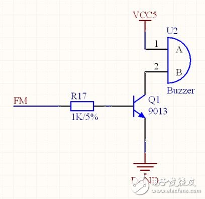
Figure 3.47 Buzzer Drive Circuit
The circuit of the eight LED indicators is shown in Figure 3.48. They are connected to the common power supply 3.3V and the other end is connected to the I/O port of the FPGA. If the output is high, the LED is off; if the output is low, the LED is lit. The interfaces of the eight LEDs are multiplexed with the segment selection signals of the digital tube.
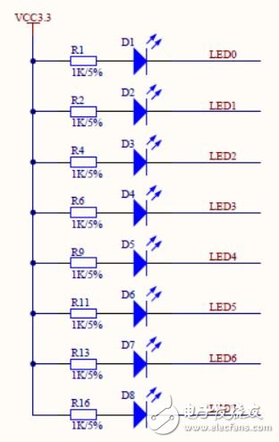
Figure 3.48 8 LED indicator circuits
The 3-digit DIP switch circuit is shown in Figure 3.49.
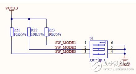
Figure 3.49 DIP switch circuit
As shown in Figure 3.50, we can compare the actual object. The default 3 DIP switches should all be dialed to the left (ie, the 1, 2, and 3 mark sides). On the circuit diagram, the VCC3.3 pull-up side. That is to say, by default, the signals SW_MODE1, SW_MODE2, and SW_MODE3 of the three I/O ports connected to the FPGA are all high. If the DIP switch is turned to the right (ie, marked ON side), the acquired input is low.
Figure 3.50 DIP switch physical photo
8 Coaxial Speaker,8 Inch Coaxial Driver,8 Inch Coaxial Speaker,8 Inch Coaxial Loudspeaker
Guangzhou Yuehang Audio Technology Co., Ltd , https://www.yhspeakers.com