MEMS manufacturing is based on semiconductor manufacturing technology; it incorporates processes such as diffusion, thin film (PVD/CVD), photolithography, etching (dry etching, wet etching) as an antecedent process, followed by thinning, Cutting, encapsulation and testing are later stages, supplemented by sophisticated inspection equipment to strictly control process requirements to achieve their design requirements.
The limit capability of the MEMS process-related equipment is also a key element to define the device size, and the mutual support between them can achieve the lowest cost of purchase. The following is a brief introduction of the features of the previous process and the equipment involved.
Diffusion process:
Diffusion in MEMS production refers to the doping of silicon (or other substrate) under certain conditions by impurities required for the process. Such as phosphorus in the silicon, boron and so on. In a broad sense, oxidation and annealing are also diffusions; the former refers to the diffusion of oxygen in SiO2 and the latter refers to the diffusion of impurities in silicon (or other substrates). The purpose is to change the electrical or chemical properties of the raw materials.
The following figure shows the diffusion furnace. The normal distribution of its three tubes (upper/middle/lower) is assigned by FATRI UTC: oxidation furnace, diffusion furnace, alloy furnace, respectively used to form SiO2, diffuse impurities, and alloy processes after bonding. .
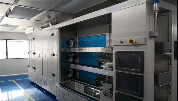
The main concern of the furnace is technical data and its usual parameters are (FATRI UTC as an example): Machinable wafer size (4†6†wafer), quartz tube maximum outer diameter (Φ 220 mm), operating temperature range ( 600°C~1200°C), Length and Accuracy of Constant Temperature Zone [Oxidation/Diffusion (900°C~1200°C 500mm/±0.5°C), Annealed Alloy (600°C~900°C 500mm/±1°C)], Temperature Rise Time (from room temperature) To 1200 °C ≤ 90min), temperature ramp capacity [maximum controllable heating rate (600 °C ~ 1200 °C 15 °C/min), the maximum cooling rate (1200 °C ~ 900 °C 5 °C/min)], feeding device [stroke ( ~1600mm), speed (30~1000mm/min), carrying capacity (≤12kg)], clean bench working level (static 100 class 10000), gas flow setting accuracy (±1% FS), gas path System airtightness (1×10⁻⁷ pa.m3/s), equipment dimensions (5270×1140×2455 L/W/H mm), power supply (three-phase five-wire ~380V 50Hz).
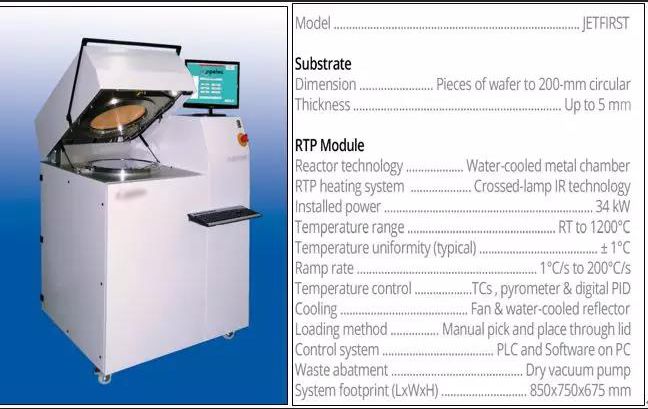
The following are RTP machine table pictures and their characteristic parameters; RTP (rapid thermal annealing) uses various thermal radiation sources to directly illuminate the sample surface and quickly heats the sample to approximately 700-1200°C in seconds to several tens of seconds. The annealing process is completed within the time; this can greatly shorten the process time.
Thin film process:
Thin film in MEMS production refers to depositing the required substances on the surface of the substrate by processes such as evaporation, sputtering, and deposition. According to the gas phase change characteristics of the process, PVD and CVD can be classified into two categories.
The PVD process involves an electron beam evaporation machine (left) and a magnetron sputtering machine (right)
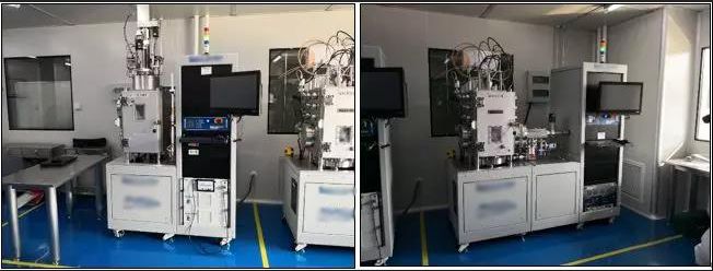
Electron beam evaporation can accurately achieve the use of high-energy electron bombardment of the helium inner membrane material by the cooperation of electromagnetic fields, so that the surface of the membrane material atoms evaporate and then deposited on the substrate; the use of FATRI UTC electron beam deposition machine in the MEMS manufacturing process, It is mainly used for vapor deposition of Pt, Ni, Au and so on.
In magnetron sputtering, an inert gas (usually Ar) is introduced under a high vacuum (10-5 Torr) and a high voltage is applied across the electrodes to generate a glow discharge. Ar atoms are ionized into Ar+ and electrons. Under the action of an electric field, Ar+ accelerates toward the target and collides with the target, sputtering a large number of target atoms, and the target atoms are deposited on the substrate. In FATRI UTC's MEMS production process, it can sputter Al, C0, Fe, alloys, etc.
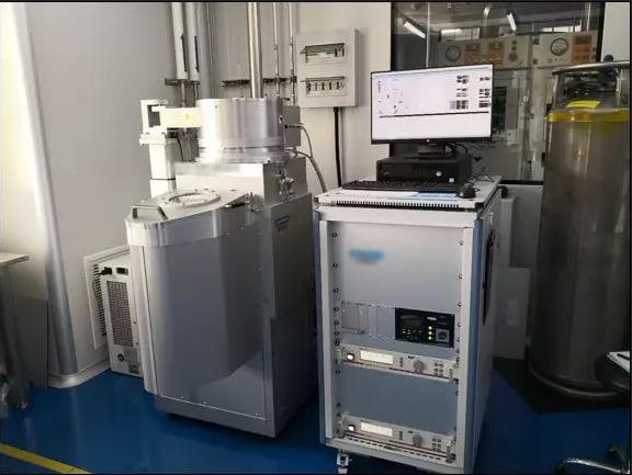
The CVD process can be subdivided into APCVD, LPCVD, and PECVD. In MEMS manufacturing, we usually use PECVD machines (see the figure below) to fabricate SiO2, Si3N4, or SiC. The process is to ionize a gas containing atoms of a thin film by microwave or radio frequency at a relatively low temperature to form a plasma locally, and the plasma is very chemically active and easily reacts, depositing a desired thin film on a substrate. .
Lithography process:
Photolithography is the selective display or masking of the film on the wafer surface and the pattern in the lithography plate through a series of production steps (mainly including gluing, exposure, and development) (the left picture shows the coating and Development machine, right exposure machine). The pattern transfer capability (minimum line width) of the lithography machine is an important indicator of the entire process line, which is directly related to the degree of integration that can be done during design. For various manufacturing centers that currently have MEMS manufacturing processes in China, the lithography machines of FATRI UTC are at a relatively advanced level.

Etching process:
In the MEMS process, etching is the use of chemical, physical or both chemical and physical methods to selectively transfer graphics on the basis of photolithography. Etching technology is mainly divided into dry etching and wet etching.
Dry etching mainly uses reactive gases and plasma for etching; for FATRI UTC, for example, ICP etching machines in MEMS manufacturing are mainly used to etch Si, Si3N4, SiO2, etc.
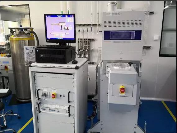
Wet etching mainly utilizes chemical reagents and chemical etching of the etched material to perform etching; taking MEMS process of FATRI UTC as an example, the wet etching of wet tank includes SiO2, Si3N4, metal, and photoresist. Etc. The cleaning step in wafer operations also needs to be performed in a wet tank.
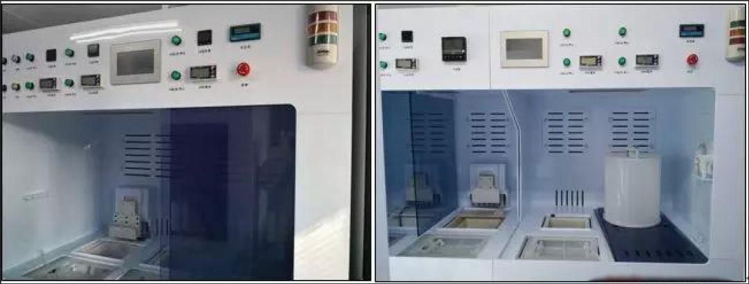
As above, in the front-end process of MEMS process (take FATRIUTC as an example), diffusion, thin film, photolithography, and etching involve diffusion furnace, RTP, electron beam evaporation machine, magnetron sputtering machine, and coating lithography development. Machine, ICP etching machine and wet tank. Each of them has its own unique role in the manufacture of the products we need with a scientific and rational combination of processes. The advantages of these products are small size, light weight, low power consumption, high reliability, high sensitivity, and ease of integration. And because it is more traditional than mechanical processing, it can be mass-produced, greatly improving the efficiency.
A live streaming screen can be a projector for both android and iPhone mobiles.we use wired and wireless projection technology to transfer the screens between mobiles and lcd screens.external devices like loudspeaker microphone digital camera lightning and others can be connected with our USB interfaces,Also PC screen projection is available for our users,with the connection of HDIM transfer interface,when you use your mobiles and PC to start a live streaming,your screens display in our live streaming screen.with our big size screen,our users can see more clearly,enlarge the distance between users and visitors,a live streaming can be with more fun and more efficiently.
Live Broadcast Movable Big Screen,Live Streaming Euqipment Movable,Projection Screen Movable Live Streaming,Live Broadcast Screen Movable Equipment
Jumei Video(Shenzhen)Co.,Ltd , https://www.jmsxdisplay.com