
[Introduction] PCB wiring is the way to connect the various devices by laying the power-on signal.
PCB wiring is the road that connects the power-on signal to connect the various devices. This is like repairing roads and connecting cars in various cities. The road construction requires one line and two lines. PCB wiring is also reasonable. It is necessary to form a two-wire loop. The low-frequency circuit is a loop. For high-speed electromagnetic fields, it is a transmission line. The most common ones are differential signal lines. Such as USB, network cable, and so on.

Differential signal lines are an ideal model for connecting device signals.
The higher the signal requirements, the closer to the differential signal line. There are a lot of board devices. If they are all wired according to different lines, the PCB area is too large, and the second is 2N lines. The workload is too large and the difficulty is very high. So people put forward a multi-layer PCB for actual needs. The concept, the most typical is the double-sided PCB board. The bottom layer is used as a common reference loop, so that the wiring only needs to be N+1, and the PCB layout is also greatly reduced.
Each layout engineer has his own way of understanding the layout. On the same PCB, different layout engineers will draw different effects. Under the premise of not affecting the performance of the PCB, the placement and layout of the components are beautiful. This is the layout. The ability of the engineer, it can be said that an excellent layout engineer is an artist!
The following picture shows the TOP silkscreen of the VPX chassis board:
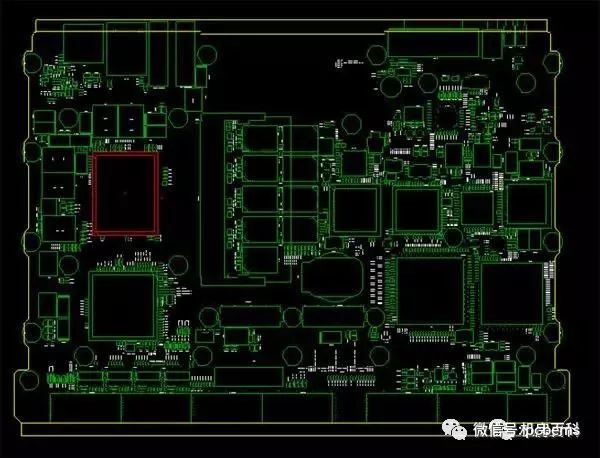
It can be seen that from the perspective of device arrangement, the filter decoupling capacitors of some chips are close to the chip. Several DDRs of the FPGA are also close to the FPGA as much as possible, and they are arranged neatly. Open the TOP layer: Is it very complicated? What about high-end?
In the final analysis, PCBlayout looks good again, the premise has to function, performance runs through, otherwise it is slag. Like this kind of system-level board, the hardware cost is tens of thousands, and the function can be realized. From the old hands, after seeing your components are imported, you can basically estimate how long the board layout takes. Cards are not the more layers, the more they are, the more layers are sometimes added to take care of sensitive signals. It is possible that there are only a few lines in one layer. Why do some people use four layers in some layers, but you use six layers? Have you considered whether the wiring length of some signals is a signal line or a transmission line, and whether it will be interfered with.
Under normal circumstances, the board priority to see whether the layout is modular, neat premise is to ensure that the sensitive signal is the priority of the overall device placement is neat, it depends on the time, the experience will be in the initial stage of the layout At that time, the direction of the sensitive signal, the layer, the first leg of the device, the direction of the resistance, the direction of the board when the board is soldered, and the influence of the device on the surrounding device when the board is out of the problem are taken into account.
Generally common silk screens, notes, test points, etc., also reflect the basic work. For those same boards that use multiple identical circuits, I just want to say that this is just a matter of adjusting the moving pitch in minutes. Where is the master's high, the same is the board, or to see who's performance is stable, the board speed is fast.
The general PCB basic design process is as follows: preliminary preparation ---- PCB structure design ---- PCB layout ---- wiring --- wiring optimization and silk screen --- network and DRC inspection and structure Check-----plate making.
The order of the PCB layout:
The wiring should be neat and uniform, and there should be no rules. These must be achieved in the case of ensuring the performance of the electrical appliance and meeting other individual requirements. Otherwise, it is a slap in the end. In the PCB design process, the wiring generally has three levels of division:
(1) First of all, it is the most basic requirement for PCB design. If the line is not laid, and the line is flying, it will be an unqualified board. It can be said that it has not yet started.
(2) The second is the satisfaction of electrical performance, which is a measure of the eligibility of a printed circuit board. This is after the connection, carefully adjust the wiring to achieve the best electrical performance.
(3) Then it is beautiful. If your wiring is connected, there is no place that affects the performance of the electrical appliances. But at a glance, in the past, if you look at the mess, plus colorful, colorful, then how good your electrical performance is, in others In the eyes, it is still a piece of garbage. This brings great inconvenience to testing and maintenance.
PCB layout principles:
(1) The key lines are as short and thick as possible, and the protected areas are added on both sides.
(2) Test points should be reserved for key signals to facilitate production and maintenance testing.
(3) Do not form a loop on any signal line. If it is unavoidable, the loop should be as small as possible; the number of vias of the signal line should be as small as possible;
(4) When transmitting the sensitive signal and the noise field band signal through the flat cable, it should be extracted by means of “ground line-signal-ground lineâ€.
(5) Pre-wire the more demanding lines (such as high-frequency lines), and the edges of the input and output ends should avoid adjacent parallel to avoid reflection interference. If necessary, ground wire should be isolated. The wiring of two adjacent layers should be perpendicular to each other, and parasitic coupling is easy to occur in parallel.
(6) The oscillator case is grounded, and the clock line should be as short as possible and cannot be cited everywhere. Below the clock oscillating circuit, the special high-speed logic circuit part should increase the area of ​​the ground, and should not take other signal lines, so that the surrounding electric field approaches zero;
(7) Use 45o of fold line wiring as much as possible, and 90o fold line should not be used to reduce the radiation of high frequency signals; (higher lines require double arcs)
(8) After the schematic wiring is completed, the wiring should be optimized. At the same time, after the initial network inspection and the DRC inspection are correct, the grounding of the unwiring area is performed, and the large-area copper layer is used as the grounding line on the printed board. It is used as a ground line to connect the place that is not used to the ground. Or make a multi-layer board, power supply, ground line each occupy a layer.
(9) Under normal circumstances, the power cable and ground wire should be routed first to ensure the electrical performance of the circuit board. Within the scope of the conditions, try to widen the power supply and ground line width. It is better to ground the ground line than the power line. Their relationship is: ground line > power line > signal line. Usually the signal line width is 0.2~0.3mm. The finest width can reach 0.05~0.07mm, and the power cord is generally 1.2~2.5mm. For the PCB of the digital circuit, a wide ground wire can be used to form a loop, that is, a ground net is used (the ground of the analog circuit cannot be used in this way)
The PCB board engineer designed the PCB board to see if it meets the following requirements. The more the number of conformances, the more the design level is:
1. The function is running normally;
2. Meet EMC test requirements;
3, PCB cost-effective;
4, layout, wiring neat and beautiful;
5. Short design time and high work efficiency;
For PCB wiring of high frequency and high current, such as switching power supply, the most taboo is that the driving signal is output with strong current and strong voltage interference. The driving signal of the MOS tube is easily affected by the output strong current. The two must maintain a certain distance, and do not rely too close. In the analog audio era, when the op amp amplification is too high, there will be a self-excited effect for the same reason as the MOS tube.
The carrier of PCB wiring is PCB board. Generally, the reference ground is near 1mm away from the PCB board, and the signal line is near 1mm from the reference ground edge. This restricts the signal to the PCB board, which can reduce EMC radiation. When there is no concept for PCB design. Just think about our daily roads, the two are exactly the same.
In short, the number and rate of PCBs alone cannot be evaluated. If the number of components is large and the signal rate is high, the smaller the area, the fewer the number of layers, and the lower the design cost. Designed and guaranteed for good electrical performance and aesthetics. Doing this is relatively powerful.

Draw-wire sensors of the wire sensor series measure with high linearity across the entire measuring range and are used for distance and position measurements of 100mm up to 20,000mm. Draw-wire sensors from LANDER are ideal for integration and subsequent assembly in serial OEM applications, e.g., in medical devices, lifts, conveyors and automotive engineering.
Linear Encoder,Digital Linear Encoder,Draw Wire Sensor,1500Mm Linear Encoder
Jilin Lander Intelligent Technology Co., Ltd , https://www.jllandertech.com