CPLDs and FPGAs are devices that we often use. Some say that there are FPGAs that configure the chip, and none of them are CPLDs; some say that the logic resources are mostly FPGAs, and the few are CPLDs; some do not distinguish directly, and they are called FPGAs. What is the difference between the two? Here we use Altera's CPLD and FPGA as an example to explain the difference between the two.
First of all, let's look at the CPLD's chip structure and figure out what parts of the CPLD are composed of. The following figure shows the chip structure of the MAX series CPLDs:

It can be clearly seen from the figure that the CPLD is mainly composed of three parts: a macro cell (a macro cell), a PIA (programmable connection), and an IO Control Block (IO control block). Each macrocell is directly connected to control signals such as GCLK (global clock) OE (output enable) GCLR (clear) and has the same delay. Each macro cell is also interconnected by a fixed length of metal wire, which ensures that the delay time of the logic circuit is fixed. The macro cell module is a logic function implementation unit of the CPLD, and is a basic unit of the device. The logic circuit we designed is specifically implemented by a macro cell. Let's take a look at the specific structure of the macro unit:
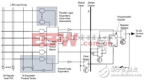
A macrocell consists of a LAB Local Array, a Product-Term Select Matrix, and a programmable D flip-flop. Each of the intersections of the logic array can be turned on through programming to achieve AND logic, and the product selection matrix can be implemented or logic. The two parts work together to achieve a complete combination of logic. The output can be selected via the D flip-flop, or the flip-flop can be bypassed. Through this structure can be found, CPLD is very suitable for combinational logic, and then with the trigger can also achieve a certain sequence of logic.
Let's take a look at the internal structure of the FPGA with the cyclone series as an example:
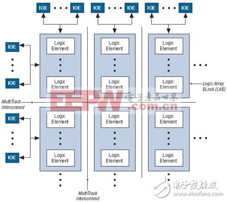
The internal of the FPGA is mainly composed of LAB units, connection lines and IO units. One LAB unit contains several LE modules. The LE module is the basic logic unit of the Cyclone FPGA. The following figure shows the specific structure of the LE module:
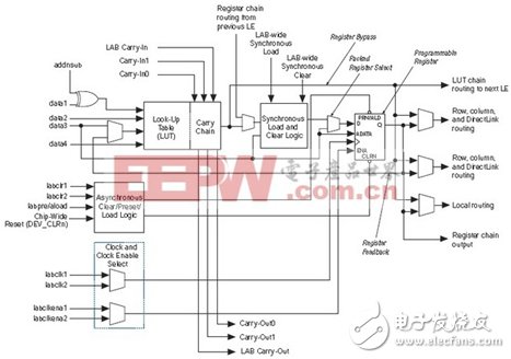
At first glance it seems more complicated, in fact, the most important part is the LUT lookup table module, and the D flip-flop behind. Others are some logic to clear the carry bypass and so on. In other words, the lookup table is the most fundamental logic unit of the FPGA. Cyclone FPGAs use a 4-input LUT lookup table. The logic we design ultimately uses EDA tools to calculate all possible results and store them in lookup tables. Each time the corresponding result is found based on the input signal, the output is then ready. In other words, the work of the FPGA is more like a RAM, and the corresponding data is output according to different input signals (addresses).
Through the comparison of the above structure, we can clearly see that CPLD is composed of real combinational circuits, and FPGA is a huge lookup table in the end! It is also this fundamental difference that has caused the difference between CPLD and FPGA. In addition to Altera, major CPLD and FPGA manufacturers include Xilinx, Actel, LatTIce, and Atmel. Each company's products have their own characteristics, and there will be slight differences in the architecture, but the basic principles are the same. Here we sort out the main differences between CPLD and FPGA:
1) The CPLD's logic array is more suitable for reprogrammable EEPROM or Flash technology. FPGAs obviously use SRAM technology more appropriately.
2) The EEPROM or Flash process determines that the CPLD has a certain number of write cycles. The actual use of FPGAs can be said to be almost unlimited configuration times.
3) Since the CPLD uses the EEPROM or Flash process, the configuration is not lost after the power is turned off, and there is no need to externally configure the chip. The FPGA uses an SRAM process and the configuration is lost after power-down. Therefore, an external configuration chip is required.
4) CPLDs are more secure. Due to the configuration of the chip, the confidentiality of the FPGA is slightly worse than that of the CPLD. Logical data may be read. (Of course FPGA chip will have some encryption measures)
5) Since CPLDs do not need to be reconfigured after power-on, they can work immediately after power-on. After the FPGA is powered on, the configuration time is required. The difference in the configuration of the logic size will also affect the configuration time.
6) Due to the continuous wiring structure of the CPLD, its timing delay is determined to be uniform and fixed. The segmented wiring structure used by FPGA causes the delay to be not fixed.
7) Due to the difference in process difficulty, the CPLD generally has a low level of integration, and is mostly a chip scale of several thousand or tens of thousands of gates. It has been difficult to achieve hundreds of thousands of gates. The FPGA is based on SRAM technology and has a higher level of integration. It can easily achieve a chip scale of hundreds of thousands of gates or even several million gates. The latest FPGA products are close to 10 million gates.
8) Also due to structural differences, CPLDs are more suitable for complex combinatorial logic, such as editing and decoding. FPGAs are more suitable for complex sequential logic. In other words, FPGAs are more suitable for trigger-rich logic structures. CPLDs are suitable for logic structures where the trigger is limited but the product terms are abundant.
9) Also due to process reasons, the general CPLD will consume more power than the FPGA.
Of course, these are just the differences between CPLDs and FPGAs. The technology is constantly evolving and these differences cannot be generalized. With the development of technology, CPLDs and FPGAs are constantly being updated.
Altera has adjusted the structure of LE in the products of StraTIx III series FPGA later, as shown below:
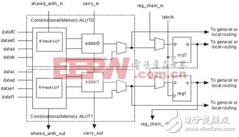
From the original 4-input lookup table plus the D flip-flop becomes two 6-input lookup tables plus two D flip-flops. Further refine the lookup table structure as follows:
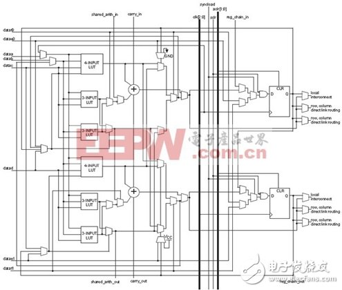
A 6-input lookup table can be subdivided into a 4-input lookup table and two 3-input lookup tables. Regardless of how the structure changes, the basic LUT lookup table approach has not changed just because of changes in resource utilization considerations. However, the new MAX II series and MAX V series CPLDs fundamentally obscure the difference between CPLDs and FPGAs. By reading the chip manual, we can see that although the names of the two series of CPLDs have not changed, the architecture is completely the same as that of the FPGA. The smallest unit has also become a LUT lookup table, and the macro unit has disappeared. It may be that the two CPLDs are able to build on the integration of the configuration circuit into the chip. In actual use, the same usage habits have been maintained with the original CPLD. It can be said that the two series of products are already FPGAs dressed in CPLD.
From the point of view of technology continuity, programmable device technology has undergone the development process of PROM-PLA-PAL-GAL-EPLD-CPLD and FPGA. CPLD and FPGA are two different development branches. Manufacturers seem to blur the distinction between CPLDs and FPGAs. Maybe there will be only a difference in the name, the two will be unified into a class of devices, or newer technologies will emerge as alternatives. Regardless of how the technology evolves, as an engineer, what we need to do is to grasp the principles, advantages, disadvantages, and application scenarios of each device, and then choose the right one in the actual project and use it flexibly.
1. Do you need to learn FPGA and CPLD at the same time?
Many students have doubts about whether or not they need to learn FPGAs and CPLDs at the same time. Ah Dong said here that there is absolutely no need to think that both FPGA and CPLD design languages ​​are Verilog. As CPLDs and FPGAs have different internal structures, they cannot be seen at the coding stage. The software will automatically generate the programming file based on the CPLD or the FPGA. Therefore, if you are learning, you can learn the FPGA by suggesting the value. If you learn the FPGA, you will use the CPLD.
2. The current circuit design scale is getting larger and larger, tens of thousands or even hundreds of thousands or even millions of register sizes. At this scale, the CPLD will not be considered at all. CPLD resources are too few.
As a mobile multi-purpose platform, tablet computers also provide many possibilities for mobile teaching. The touch-based learning & entertainment teaching platform allows children to efficiently improve their academic performance in a relaxed and pleasant atmosphere. Such tablet computers generally integrate two learning sections of various courses and systematic learning functions. Generally, it includes multi-disciplinary high-quality teaching resources. The education tablet has the following main functions: it has the functions of touch screen input, text editing, picture editing, data storage, data management, wired and wireless Internet access that ordinary tablet computers have; Management functions, search methods support manual search, query by keyword, query by time; text and pictures can be scanned and converted into documents to save.
Education Tablet,learning tablet,leaning machine,New learning tablet
Jingjiang Gisen Technology Co.,Ltd , https://www.jsgisentec.com