PLD (Programmable Logic Device) is a general term for programmable logic devices. Most of the early PLDs belonged to the EEPROM or Product Term structure. FPGA (Field Programmable Gate Arry) refers to the online programmable logic array, first introduced by Xilinx. Mostly SRAM framework or look-up table framework, EPROM download for external configuration. Xilinx refers to the SRAM framework or the look-up table framework, and the PLD downloaded by the EPROM for external configuration is called FPGA. The PLD of the Flash, EEPROM framework or product term frame is called CPLD. Altera refers to its PLD product series MAX/FLEX/ACEX/APEX series as CPLD. Since the FLEX/ACEX/APEX series are also SRAM type, EPROM downloads for external configuration are required. Many people refer to Altera's FLEX/ACEX/APEX series products as FPGAs.

Programmable logic device (PLD) is an epoch-making new logic device developed on the basis of ASIC design in the 1970s. Since the advent of PLD devices, TTL, CMOS, ECL, and static RAM technologies have been used in the manufacturing process. The device types are PROM, EPROM, E2PROM, FPLA, PAL, GAL, PML, and LCA. The development of PLD in terms of performance and scale depends mainly on the continuous improvement of manufacturing process. High-density PLD is the product of the high development of VLSI integration process. In the late 1980s, ALTERA and XILINX used EECMOS technology to introduce large-scale and ultra-large-scale complex programmable logic devices (CPLDs) and field-programmable logic gate array devices (FPGAs). This chip achieves high integration, and its application flexibility and multi-configuration functions are unmatched by previous LSI/VLSI circuits. Since the 1990s, programmable logic devices CPLD/FPGA have been rapidly developed, moving toward high integration, high speed and low price; not only with electrical erasing, but also for edge scanning and online programming. Advanced features; its application field is expanding, it can be used in state machine, synchronization, decoding, decoding, counting, bus interface, serial-to-parallel conversion, etc., and its application in signal processing field is also active. Using CPLDs can increase system integration, reduce noise, increase system reliability, and reduce costs.
This article mainly introduces the characteristics and applications of ATMEL's CPLD chip ATF1508AS. The ATF1508AS is a high-performance, high-density complex programmable logic device (CPLD) implemented using ATMEL's proven electrical erasing technology. It is fully compatible with ALTERA's EPM7000 series pins; it can convert the EPM7000's POF file into an industry suitable for the ATF1508AS. Standard JEDEC programming files are downloaded to the ATF1508AS chip.
1 Features of ATF1508AS
The ATF1508AS is a high-performance, high-density complex programmable logic device (CPLD) that utilizes ATMEL's proven electrical erasing technology. With 128 logical macro units and a maximum of 100 inputs, it easily integrates the logic functions of a range of TTL, SSI, MSI, LSI and legacy PLDs. The ATF1508AS's enhanced routing switch matrix adds the number of gates available and the success rate of pin locks when design changes, which is very important. The ATF1508AS has 96 bidirectional I/O pins and 4 input pins. These four input pins can also be used for global control signals, global register clocks, global resets, and global output enable.
Each of the 128 macrocells generates a hidden feedback loop to the global bus, and each input pin and I/O pin are also fed into the global bus. The switch matrix of each logic block selects 40 separate signals from the global bus, and each macrocell also generates a return logic entry to the local bus. Cascading logic between macrocells enables complex logic functions to be implemented quickly and efficiently. The ATF1508AS includes eight such logical chains, each of which can be summed by logically fanning up to 40 product terms.
The ATF1508AS is an in-system programming (ISP) device. It is fully compatible with JTAG's Boundary Scan Description Language (BSDL) using the industry standard 4-pin JTAG interface (IEEE Standard 1149.1). The ISP allows the device to be programmable without being removed from the printed circuit board; in addition to simplifying the production process, the ISP also allows design modifications through software.
The pin-hold circuit of the ATF1508AS provides settings for all input and I/O pins. When any pin is driven high or low, the pin will remain in the previous high or low state immediately after the pin is left floating. This circuit prevents unused input and I/O lines from floating and becomes intermediate voltage values, which can result in unnecessary power consumption and system noise. The pin-hold circuit removes the need for external pull-up resistors and DC power dissipation.
The encryption feature of the ATF1508AS protects the design of the ATF1508AS. The two-byte (16-bit) user signal can be accessed by the user, and can store the project name, part number, version or date, etc., and the access of the user signal is not affected by the state of the encrypted fuse.
The ATF1508AS has a power-on reset feature. During power-up, all I/O pins will be tri-stated until VCC reaches the power-up voltage, which prevents bus contention during power-up. The registers of the ATF1508AS are designed to be reset on power-up. A small delay from VCC to VRST, all registers will be reset to low level, and the output state will be set according to the polarity of the buffer. This feature is critical to the initialization of the state machine.
2 macro unit of ATF1508AS
The macro unit of ATF1508AS is shown in Figure 1. Its macro unit is flexible enough to support high complex logic functions and work at high speeds. The macrocell consists of five parts: a product term and a product term selection multiplexer, or an exclusive OR/cascade logic, a flip-flop, an output selection and enable, and a logic array input. Unused macrocells can be disabled by the compiler to reduce power consumption.
(1) Product term and product term selection matrix
Each macrocell has five product terms, each of which receives all signals from the global bus and the local bus as its input. The product term selection matrix (PTMUX) allocates these 5 product terms to the logic gates of the macrocells as needed, and is also responsible for assigning control signals. The programming of the product term selection matrix is ​​determined by the design compiler, which will select the optimized macro cell configuration.
(2) or / XOR / Cascade Logic
The logical structure of the ATF1508AS is designed to effectively support all logic. Within a macrocell, all product terms can be placed into an OR gate to produce a 5-input and/or summation term. Fanning additional product terms through adjacent macrocells can be extended to 40 product terms with only a small delay. The XOR gate of the macrocell allows for efficient comparison and arithmetic functions, where one input to the XOR gate is derived from the summation of the OR operation, and the other input can be a product term or a fixed high or low level. For combinatorial logic outputs, fixed levels allow for polarity selection; for sequential logic, fixed levels allow the use of inversion rules (inferred by Morgan's Law) to simplify product terms. XOR gates can also be used to simulate T- and JK triggers.
(3) Trigger
The triggers of the ATF1508AS have very flexible data and control functions. The input to the trigger can come from an XOR gate, a separate product term, or directly from the I/O port. Selecting a separate product term allows a hidden register feedback to be generated in a combinatorial logic output macrocell (this feature is automatically implemented by the fitter software). In addition to the D, T, JK, and SR types, the ATF1508AS's flip-flops can also be configured as latches. In this mode, data passes when the clock is high and latches when the clock is low.
The clock signal can be a global CLK signal (GCK) and a separate product term. The flip-flop changes state on the rising edge of the clock. When the GCK signal is used as a clock signal, a product term of the macrocell can be selected as the clock enable signal. When the clock enable function is used, when the enable signal (product term) is low, all clock edges are ignored. The asynchronous reset signal (AR) of the flip-flop can be a global reset signal (GCLEAR), a product term or not used. AR can also be the logical or output of GCLEAR and a product term. The asynchronous set signal (AP) can be a product term or not used.
(4) Output selection and enable
The output of the ATF1508AS macrocell can be selected as a register type and a combination type. The hidden feedback signal can be a combination or register signal regardless of whether the output is a combined or a register type. The Output Enable Multiplexer (MOE) controls the output enable signal. Any buffer can be permanently enabled if it is a simple output operation. If the pin is used as an input, the buffer can also be permanently disabled. In this configuration, all macrocell resources are still available, including hidden feedback signals, expanders, and cascading logic. A global output enable signal can be selected for each macro unit's output enable signal. The device has six global output enable signals (OE).

(5) Logic array input
The logic array inputs include the global bus/switch matrix and the return bus:
全局 Global bus / switch matrix
The global bus includes all input and I/O pin signals as well as hidden feedback signals for all 128 macrocells. The switch matrix of each logic block takes all of the signals of the global bus as its inputs. Up to 40 of these signals can be selected as inputs to the logic block under the control of the software.
è¿” Return bus
Each macrocell can generate a return product term. This signal is connected to the local bus and is valid for 16 macrocells, which is the inverse polarity of a product term of the macrocell. The 16 return items for each local bus allow for the generation of high fan-in summation terms (up to 21 product terms) with only a small delay.
3 design software support
ATMEL provides design software for CPLD, and many third-party tools also support the design of ATF1508AS, which can be logically described in a variety of advanced description languages ​​and formats, such as CUPL, ABEL, VHDL, etc. Because the ATF1508AS is fully pin-compatible with ALTERA's EPM7000 series, ALTERA's MAXPLUSII software can be used. It can compile and synthesize VHDL language, which is easy to use and powerful. MAXPLUSII combines to produce a POF file suitable for ALTERA's CPLD programming. Using POF2JED software (provided by ATMEL), the POF file can be converted to an industry standard JEDEC programming file suitable for ATF1508AS and downloaded to the ATF1508AS chip.
4 device programming
The ATF1508AS device is in-system programming (ISP) using the 4-pin JTAG protocol. ATMEL provides ISP hardware (download cable) and software to allow programming of the ATF1508AS from a PC. To allow ISP programming to support Automated Test Set (ATE) vectors, serial vector format (SVF) files must be generated by ATMEL's ISP software, or converted to other ATE test formats than SVF. The ATF1508AS device can also be programmed with a standard third-party programmer, where the JTAG ISP port can be disabled allowing the four additional I/O pins to be used for logic functions.
Another feature of the ATF1508AS is that if the programming process is interrupted for any reason, the device will be locked to prevent the input and I/O pins from being driven. In this state, the input and I/O pins default to a high-impedance state. The input and I/O pins will also be in a high-impedance state when programming the device. In addition, the pin hold circuit settings will remain in the previous state during device programming. The ATF1508AS device is initialized to an erased state at the factory and can be used directly for ISP programming.
5 application examples
(1) Apply ATF1508AS for serial-to-parallel conversion
This system uses ATMEL's ATF1508AS for serial data to parallel data conversion. In the data acquisition, the 24-bit high-precision Σ-Δ analog-to-digital converter CS5321/CS5322 components produced by Crystal Semiconductor are used. The component finally outputs a serial digital signal with a 2-bit complement format of 24 bits, which can be converted to parallel data for easy interface with the microcontroller. The serial-to-parallel conversion can be implemented using a shift register. For 6-channel 24-bit sampling, if a shift register is used, an 8-bit shift register is required, which is 3&TImes; 6=18, and several decoders are used. In this way, the number of chips will increase greatly, occupying a large area of ​​the board, and the volume of the system will increase. The system uses ATF1508AS to achieve 6-channel 24-bit data serial-to-parallel conversion, which integrates most digital logic designs (including combinatorial logic and sequential logic) into one chip, greatly reducing the number of chips and reducing system size.
Since there are 128 macro cells in the ATF1508AS and 24 shift registers are required for 24-bit serial-to-parallel conversion, it is not possible to perform 6-channel serial-to-parallel conversion at the same time, which can only be time-multiplexed. The system performs serial-to-parallel conversion in three times, each time converting two channels, waiting for the one-chip computer to read the parallel data of two channels, and then performing the remaining conversion. The partial serial-to-parallel conversion VHDL program is as follows (the hardware description language is VHDL, the software is ALTERA's MAXPLUSII software and ATMEL's POF2JED software, the download software is ATMEL's ATMISP, and the download cable is ATMEL's dedicated cable):
S2p : process(SCLK1M, DRDYIN, WORKING, RESET)
Begin
If WORKING='1' or RESET='1' then
Shift_enable <<= '0';
State "= s0;
Elsif SCLK1M'event and SCLK1M='0' then
Count1 <<= count1+1;
Case state is
When s0 =》if DRDYIN='0' then
Shift_enable <<= '1';
Count1 <<= (others=》'0');
Int_reg "= '1';
State "= s1;
Elsif READOK='1' then
Int_reg "= '1';
End if;
When s1=â€shift_reg0â€==shift_reg0(22 downto 0)& SOD(0);
Shift_reg1"=shift_reg1(22 downto 0)& SOD(1);
If count1=23 then
Shift_enable <<= '0';
Int_reg <<= '0';
State "= s2;
Else
Int_reg "= '1'; end if;
When s2 =》 if shift_enable='1' then
Shift_reg0"=shift_reg0(22 downto 0)& SOD(2);
Shift_reg1"=shift_reg1(22 downto 0)& SOD(3);
If count1=23 then
Shift_enable <<= '0';
Int_reg <<= '0';
State "= s3;
Else
Int_reg "= '1'; end if;
Elsif READOK='1' then
Shift_enable <<= '1';
Count1 <<= (others=》'0');
End if;
When s3 =》if shift_enable='1' then
Shift_reg0"=shift_reg0(22 downto 0)& SOD(4);
Shift_reg1"=shift_reg1(22 downto 0)& SOD(5);
If count1=23 then
Shift_enable <<= '0';
Int_reg <<= '0';
State "= s0;
Else
Int_reg "= '1'; end if;
Elsif READOK='1' then
Shift_enable <<= '1';
Count1 <<= (others=》'0');
End if;
End case;
End if;
End process;
(2) Application of ATF1508AS for high-speed USB communication
USB is a new interface technology applied in the field of PC in recent years. It has the characteristics of convenient use, fast speed, flexible connection and hot plugging. The USB 1.1 protocol defines a transmission speed of 1.5 Mb/s at high speeds of 12 Mb/s and low speed. To achieve a high speed of 12 Mb/s (equivalent to nearly 1 MB/s), it takes about 1 μs to transfer 1 byte. However, due to the control transfer of USB, error detection, and the speed limit of the microcontroller itself, it is difficult to achieve such a high speed. Therefore, DMA mode must be used to achieve true high-speed transmission, and similar DMA mode can be realized by using CPLD. The MCU is responsible for interpreting the control transfer of the USB. When the number of external accesses is sent to the USB interface chip, the MCU gives up the bus and the CPLD completes the work. The CPLD generates the read timing and address of the external memory, the chip select signal, and simultaneously generates the write timing and address of the USB interface chip, and the chip select signal, so that the external memory data can be automatically realized to the USB interface chip, and the speed is fast. No microcontroller intervention is required. The following is a VHDL program fragment for RAM read timing, address signals, and USB interface chip write timing:
Rram1 : process(SCLK2M) -- RAM_OE (RAM read timing)
Begin
If SCLK2M'event and SCLK2M='1' then
If read='0' then
Ram_oe_reg <<= '1';
Cpld2_counter <<= (others=》'0');
Elsif read='1' then
Cpld2_counter <<= cpld2_counter+1;
If cpld2_counter》0 then
Ram_oe_reg "= not ram_oe_reg;
End if;
End if;
End if;
End process;
Rram2 : process(SCLK2M, WORKING, RESET) -- ADDRESS (RAM address signal)
Begin
If WORKING='1' or RESET='1' then
Adr_reg "= (others=》'0');
Elsif SCLK2M'event and SCLK2M='0' then
If read='1' and ram_oe_reg='1' and cpld2_counter》2 then
Adr_reg "= adr_reg+1;
End if;
End if;
End process;
Wd12 : process(SCLK2M) -- USB chip read timing
Begin
If SCLK2M'event and SCLK2M='0' then
If read='0' then
D12_wr_reg <<= '1';
Elsif read='1' and cpld2_counter/=129 then
D12_wr_reg "= not d12_wr_reg;
End if;
End if;
End process;
Conclusion
The advantages of CPLD devices are shortening the development and production cycle, and the flexibility of the field is good. With the development of electronic technology, the integration degree is getting higher and higher, the speed is getting faster and faster, and the price is gradually decreasing, so the market is developing rapidly. ATMEL's ATF1508AS is a high-performance, high-density complex programmable logic device that is easy to use and has a high price/performance ratio, so it has broad application prospects.
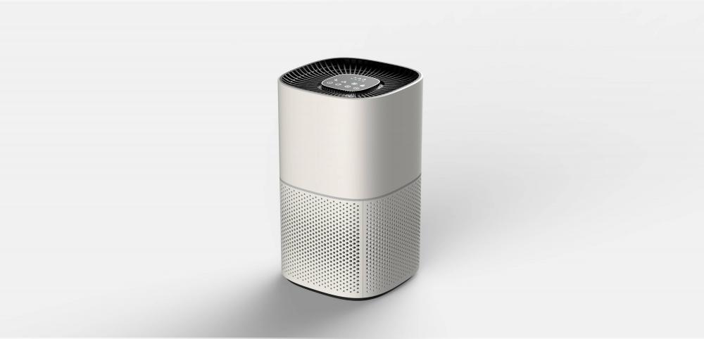
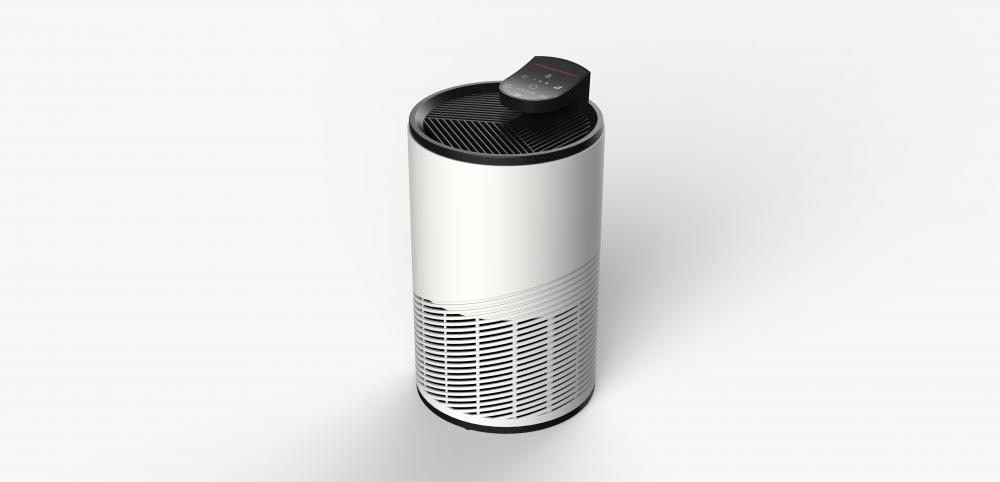

KYFEN air purifier with HEPA filter H13 active carbon, 3 stages Filtration, The primary filter intercepts large particles such as hair and dust. The second layer of high-quality filter, can remove nano level of tiny particles, and also can effectively block some bacteria and viruses. The third layer of high quality activated carbon, can effectively adsorb formaldehyde and other harmful substances, effectively remove the odor in the air. Efficient filtering bacteria and viruses, filter out a variety of bacteria, The sterilization rate is up to 99.9%. The high efficiency air pressurization system designed by us makes the air purifier achieve small volume and high performance, with CADR value up to50~200m3/h and applicable area of 6~23m2.
Touch screen operation panel, 3 Fan speeds, the classic tower structure design can make efficient use of the body space, so that the small body carries a stronger purification capacity. The additional 943 air inlet holes make the air inlet space wider and form a three-dimensional circulation purification style.
Air Purifier,Air Cleaner,Air Purifier For Home,Small Air Purifier
CIXI KYFEN ELECTRONICS CO.,LTD, , https://www.kyfengroup.com