Analog-to-digital converters (also known as ADCs) are widely used in a variety of applications, especially those that need to process analog sensor signals, such as data acquisition systems that measure pressure, flow, speed, and temperature, to name a few. In general, these signals are time domain signatures that appear as pulses or step functions.

In any design, it is always important to understand the total system accuracy of these types of applications, especially those that require minimal sensitivity and variation in the waveform. Ideally, each volt applied to the input of the signal chain is digitally represented by the ADC as one volt output. But that is not the case. There is a finite amount of error associated with this in all converters and signal chains.
This article describes the errors associated with the analog to digital converter itself. This article will also reveal to what extent the inaccuracy of the internals of the converter will accumulate. When defining the system parameters of a new design, if the measurement accuracy is extremely important, then these contents are important for understanding how to correctly designate an ADC. Finally, this article will discuss a simple error analysis to help select the right converter for your design.
ADC inaccuracy
Regardless of the signal chain, the converter is an essential element of the system. Any ADC selected for the design will determine the overall accuracy of the system. In other words, the system accuracy cannot be higher than the least significant bit (LSB) size of the converter. To illustrate this, let's look at a short guide to ADC inaccuracy.
First, notice that because ADCs are not ideal and have limited resolution, they can only display a limited amount of information representation at the output. The amount of information represented is represented by the converter's full-scale input divided by 2N, where N is the ideal number of bits for the converter.
For example, assuming a 12-bit ADC is selected, it can represent any signal applied to the converter input at 4096 digits at the output. These representations do have a finite amount of error. Therefore, if the 12-bit ADC has an input full-scale (VFS) of 10 V pp, then the ideal LSB size is 2.44 mV pp with an accuracy of ±1.22 mV.

Formula 1
In fact, the ADC is not ideal. There is some noise inside the converter,

There is even noise in the DC. Remember that a 1 kΩ resistor is equivalent to 4 nV∙ Hz (1 Hz bandwidth, 25 °C). Note that when viewing a 12-bit ADC data sheet, the SNR is typically approximately 70 dB to 72 dB. However, a 12-bit ADC should ideally have 74 dB according to the following formula:

Formula 2
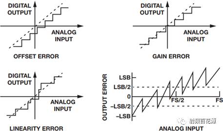
Therefore, the 12-bit resolution is actually unachievable because the converter itself has some inaccuracy, as shown in Figure 2.
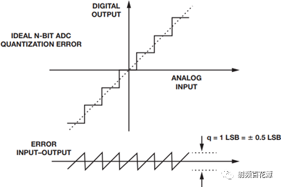
These inaccuracies or errors determine the efficiency of the converter's representation of the signal and are ultimately received by the signal chain. The offset error is defined as the analog value of the transfer function that cannot pass the zero point. The gain error is the difference between the full-scale values ​​between the ideal and actual transfer functions when the offset error is zero. The linearity error or non-linearity in the usual sense refers to the linear deviation between zero level and full scale, as shown in Figure 1.

Figure 1. ADC quantization error

Figure 2. ADC inaccuracy
More information about ADC inaccuracy
After defining and understanding the most basic analog-to-digital converter errors, it is helpful to explain the difference between these errors. Most of the ADC's offset and gain have such small errors that can usually be ignored or adjusted (cancelled) by an external analog circuit, or corrected using digital techniques. However, other errors such as linearity, quantization, and temperature coefficients cannot be easily adjusted or eliminated.
The linearity of the analog-to-digital converter is only relevant to the converter itself, depending on the architecture and process variations. There are many ways to correct it, but they are all expensive. Designers have two choices: buy better, more expensive converters, or digitally correct linearity. The cost of digital correction is also very high. This means that more resources may be needed to specify the DSP or FPGA because the linearity will change with temperature and process variations. Depending on the sampling rate, IF, and resolution, digital corrections may require extensive feature representations and lookup tables to instantly correct or adjust the performance of the ADC.
There are two types of errors in linearity: they are differential nonlinearity and integral nonlinearity, often referred to as DNL and INL, respectively. DNL is defined as any error or deviation from the ideal value. In other words, it represents the deviation between the analog difference of two adjacent codes and the ideal code value VFS/2N. Think of it as a factor related to the SNR performance of the ADC. As the deviation of the code grows larger, the number of conversions also decreases. The error is within ±0.5 LSB over the temperature range and is guaranteed to be free of missing codes.
INL defines the ideal linear approximation curvature deviation between zero level and full scale. In most cases, INL determines the SFDR performance of the ADC. The INL total deviation shape determines the most important harmonic performance. For example, an INL curve that bows will produce a worse even harmonic, and an INL curve that is S-bow usually produces odd harmonics. This error is essentially frequency dependent and independent of such error analysis.
Even if the static offset and gain errors can be eliminated, the temperature coefficient associated with the offset and gain error will still be present.
For example, a 12-bit ADC has a 10 ppm gain error, or FSR/°C = 0.001%/°C.
The 1 LSB in a 12-bit system is 1â„4096, or approximately equal to 0.024%.
Therefore, if 125°C Δ (–40°C to +85°C), a ±2.5 LSB gain temperature coefficient error is produced, or 0.001% × 125 = 0.125%. .
Among them, 0.125/0.024 = 5.1 or ±2.55 LSBs.
For offset tempco a 5 ppm offset error or FSR/°C = 0.0005%/°C.
This will produce a ±1.3 LSB offset temperature coefficient error, or 0.0005% × 125 = 0.0625. Among them, 0.0625/0.024 = 2.6 or ±1.3 LSBs.
ADC error analysis
Other sources of error that affect converter performance are: CMRR, clock jitter, inherent board noise, coupling, and more. All of these errors ultimately determine how effectively the ADC represents the signal; usually the ADC can represent itself more efficiently in the frequency domain.
From a time domain perspective, analyzing the total accuracy of the converter requires understanding the following five errors:
Relative accuracy DNL, ​​defined as ±0.5 LSB
The relative accuracy temperature coefficient and the DNL temperature coefficient are usually included in the relative accuracy specifications of the data sheet.
Gain temperature coefficient error is ±2.5 LSB (data from the example above)
Offset temperature coefficient error, ±1.3 LSB (data from the example above)
Power supply sensitivity, usually expressed as the low frequency PSRR (power supply rejection ratio) in the first Nyquist zone. For a 12-bit ADC, it can generally be expressed as 60 dB or ±2 LSB.
Only square and root (RSS) operations are required, all of which form a ±3.5 LSB total converter error. This result may be too pessimistic. However, the statistical tolerance results may be too optimistic, or the sum of the total errors divided by the number of errors, ie (0.5 + 2.5 + 1.3 + 2) / 4 = ± 1.58 LSBs. The actual ADC tolerance should be between these two ideas or methods.
Therefore, when adding precision errors to the converter, or performing any system accuracy analysis, the designer should use the weighted error source method and then perform RSS calculations on these error sources. This is the best way to determine the total error of the ADC. Therefore, the relative accuracy of ±0.5 LSB should be kept at 100%. However, the ±2.5 LSB gain temperature coefficient error should be 66% of the total error, or 2.5/(0.5 + 1.3 + 2) × 100. The offset temperature coefficient error of ±1.3 LSB will be 26% of the total error, or 1.3/(0.5 + 2.5 + 2) × 100. The power supply sensitivity error of ±2 LSB will be 47% of the total error, or 2/(0.5 + 1.3 + 2.5) × 100. Add these weighted errors in RSS or calculate the square root √((0.5 × 1)2 + (2.5 × 0.66)2 + (1.3 × 0.26)2 + (2 × 0.47)2) The total error is ±2.0 LSB, this is a more realistic result, between the optimistic approach and the pessimistic approach above.
ADC bandwidth accuracy
The ADC also has time-of-set precision. Remember that the converter's internal front end needs to have enough bandwidth (BW) to accurately sample the signal. Otherwise, the cumulative error will be greater than the results discussed above.
In general, the internal front end of an ADC needs to be established (0.5/Fs) in a half cycle or sample clock cycle to provide an accurate representation of the internal analog signal capture. Therefore, for a 12-bit ADC with a sample rate of 2.5 GSPS and a full-scale input range of 1.3 V pp, the full power bandwidth (FPBW) can be derived from the following transient equations:

Solve t:

Substituting τ = 1/(2 × π × FPBW), a time constant, solves FPBW:

Now, let t = 0.5/Fs, then the time required for sample setup is as follows (sample period is 1/Fs):

This will minimize the bandwidth or FPBW required for the internal front end of the ADC. This is the bandwidth required for the internal front end of the converter to settle to within 1 LSB and properly sample the analog signal. To meet the 1 LSB accuracy requirements of this type of ADC, this would take several time constants.
A time constant is 24 ps or τ = 1/(2 × π × FPBW). To find out the number of time constants required to reach the LSB size requirement within the ADC's full-scale range, you need to find the full-scale error or %FS. Or 1 LSB = FS/(2N), where N = number of bits, or 1.3 V pp/(212) = 317 μV pp, and %FS = (LSB/FS) × 100 = 0.0244.
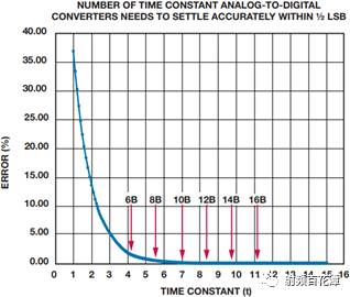
By plotting the Euler number or eτ, a curve can be drawn so that the relative error can be easily seen by each constant. As can be seen in Figure 3, it takes 8.4 time constants for the 12-bit ADC sample to be built up to approximately 1 LSB.

Figure 3: Establishing the relationship between precision and time constant
This allows the designer to estimate the maximum analog input frequency or sampling bandwidth for the converter and still builds up to 1 LSB error. Beyond this range, the ADC cannot accurately represent the signal. This can be simply defined as: FMAX = 1/(τ × number of time constants) or 1/(24 ps × 8.4) = 4.96 GHz.
Remember, this is the best case and assumes a single pole ADC front end. Not all real-world converters work this way, but it's a good place to start. For example, the model described above can be applied up to 12 bits, but for 14/16 bits and higher, a second-order model needs to be used based on these subtle effects to extend the settling time beyond the predicted first-order model.
A brief description of the ADC bandwidth
Keep in mind that the full power bandwidth of the ADC is different from the available bandwidth or sampling bandwidth of the converter as defined above. It can be used as the full power bandwidth (FPBW) of an analog signal input op amp. The signal is more like a triangular wave signal and there is a lot of distortion at the output. The FPBW is the bandwidth required for the ADC to accurately capture the signal and properly establish the internal front end (6.62 GHz in the previous example). It is not a good idea to choose an IF and use the converter within this range because the performance results of the system will change dramatically; at approximately 5 GHz, as shown in the example above, according to the nominal resolution and performance specifications in the converter data sheet The full-scale bandwidth is much higher than the converter's own maximum sampling bandwidth. The design is built around the sampling bandwidth. All designs should avoid using one or all of the highest frequency fractions of the rated full power bandwidth, otherwise the dynamic performance (SNR/SFDR) will drop and vary significantly. In order to determine the sampling bandwidth of a high speed ADC, the example above should be used as it is not always available from the data sheet. Typically, the data sheet will specify and even list the frequency at which the converter's sampling bandwidth is production tested to ensure rated performance. However, in older ADC products these test frequencies are not always defined in FMAX as data sheets. These bandwidth terms in the industry need to be better explained, defined and tested in the future.
in conclusion
This article gives guidance on how to look at inaccuracies in general static ADCs and ADC inaccuracies in bandwidth. A more in-depth explanation of the ADC errors and how these errors affect the signal chain is also provided. Keep in mind that not all components are built in the same way, which is true for both active and passive components. Creating an electronic watch that encompasses all of these errors is a convenient way to insert different signal chain components, allowing for faster evaluation and determining component trade-offs. This is especially true for trade-offs between cost, size, and power consumption between components and for measuring signal chain performance differences.
Magnetic Ring Inductors,High Current Manganese Zinc Toroidal Inductors,Manganese Zinc Magnetic Ring Inductor Power,Toroidal Plug-In Inductors
Shenzhen Sichuangge Magneto-electric Co. , Ltd , https://www.scginductor.com