Leakage current refers to the current formed between the metal parts insulated from each other in the electrical equipment, or between the live parts and the grounded parts, through the surrounding medium or the insulating surface, in the absence of a voltage applied by the fault. It also includes the current that the device passes through the body to reach the earth or the current that is returned to the device by the device when the person touches the electrical device. It is one of the important indicators to measure the insulation of electrical appliances, and it is also the main indicator of product safety performance. The leakage current test system should internally simulate a human body electric shock according to different standards, or the most suitable physical impedance of the human body, with one or several sets of circuits consisting of specific impedance values ​​and resistors and capacitors that meet certain power requirements. The current flowing through the body impedance network is measured by connecting the body impedance network to the instrument component to be tested that may be electrically shocked by the human body.
System hardware design
The measurement and control system consists of PC, DSP chip TMS320F2812 control system and peripheral extended function circuit, leakage current acquisition signal conditioning circuit, DSP and PC communication interface circuit, collecting, calculating, displaying and storing to analyze the leakage current characteristic value of the tested instrument.
Highly amplified and linear isolated circuit design
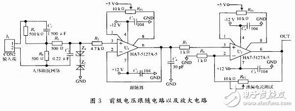
According to the latest standard requirements for leakage current testing, it is required to detect leakage currents from 50 Hz to 1 MHz. Therefore, the frequency range of the amplifier is very high. This paper selects the low noise precision operational amplifier HA7-5127-5, which has a passband bandwidth of 8.5 MHz, which meets the requirements of more than 1 MHz. The front voltage follower circuit and the amplifier circuit are shown in Figure 3.

In the figure, the leakage current of the device under test passes through a single analog body impedance network, which converts the current signal into a voltage signal, and the clamp diode circuit acts as a protection to prevent the positive and negative voltages from being too high. After adding the follower amplifier U1 to match the impedance and stabilize the signal, the amplifier U2 amplifies the weak leakage current signal, and adjusts the amplification gain of the circuit through RP1 for observation and acquisition.
In the leakage current isolated data acquisition circuit, the signals to be isolated are ADC control signals (DC level) and ADC working clock signals (signals of several megabits or higher). Under such application conditions, if ordinary optocouplers are used. Isolation devices can only isolate DC or low frequency signals, so optocoupler technology is difficult to meet the need for leakage current isolation. The magnetic coupling isolation device cannot transmit the low frequency signal and the direct current signal, and the magnetic coupling isolation has good transmission performance to the digital signal, and even if the analog signal is transmitted, the signal distortion is caused. The solution is to power the analog signal that needs to be transmitted. The flat rise is such that the minimum current value of the analog signal can drive the isolation device to work, and the distortion of the transmitted signal is guaranteed. Another solution is to modulate the low-frequency signal to be transmitted to the high-frequency carrier, and then use the magnetic coupling isolation circuit to isolate the transmission. At the receiving end, the low-frequency signal is extracted by the demodulation circuit, which can be transmitted by the magnetic coupling isolation circuit. The purpose of the low frequency signal. The novel magnetic coupling isolation circuit designed in this paper can realize the magnetic coupling isolation transmission of low frequency and DC signals without modulation and demodulation circuits, and the circuit structure is simple, the power consumption is small, and the signal transmission delay is small.
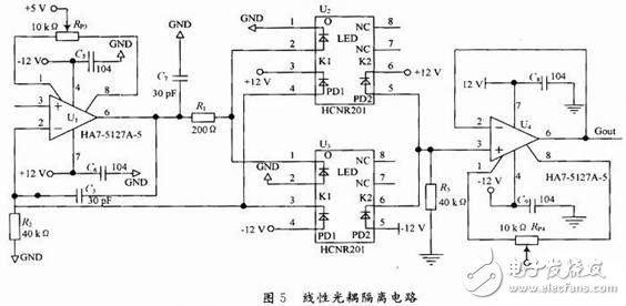
In this paper, the isolation is performed by analog isolation amplifier to achieve electrical isolation between the test system and the measured object. The high linearity analog optocoupler HCNR201 is selected. The main parameters are as follows: ±5% transmission gain error and ±0.05% Linearity error; with a bandwidth greater than 1 MHz; input voltage range is 0 to 15 V. The circuit is shown in Figure 5.

Circuit Description: Optocoupler U2 is used for isolation of positive polarity signals, and optocoupler U3 is used for isolation of negative polarity signals. In the isolated circuit, R2 adjusts the magnitude of the bias current of the primary op amp U1 input, and C3 acts as a feedback, and at the same time filters out the glitch in the circuit to avoid the accidental impact of the aluminum gallium arsenide LED of the HCNR201. R1 can control the luminous intensity of the LED, thus controlling the channel gain. The HC-NR201 is current driven and requires an operating current of 1 to 20 mA. Because it is an isolated bipolar signal, the dual-supply HA7-5127-5 op amp has an output current of 25 mA. R3 is a sampling resistor that converts the optocoupler output current into a voltage signal, and forms a voltage follower circuit with the operational amplifier U1 to achieve impedance matching between the input and output circuits. In the linear optocoupler circuit of FIG. 5, the isolation voltage gain of the isolation circuit, the isolation gain of the isolation circuit is only related to the resistance values ​​R3, R2, and is independent of the current transmission characteristics of the optocoupler, thereby achieving voltage isolation.
Level raising circuit design
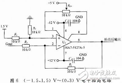
Since the A/D sampling range integrated in the TMS320F2812 is 0~3 V, the gain of the amplifier can be adjusted before the acquired signal is optocoupled, so that the collected voltage signal falls within the range of -1.5 to +1.5 V. Then, design a +1.5 V reference voltage source to raise the level of the acquired signal, so that the sampling signal can be guaranteed to be in the range of 0 to 3 V. The circuit is shown in Figure 6.

The purpose of level raising is achieved. The value range of Ui is -1.5 to +1.5 V, and the range of Uo is 0 to 3 V. At this time, the acquired signal is within the input voltage range of 0 to 3 V, which satisfies the requirements.
Pvc Trunking,Pvc Cable Trunking,Plastic Cable Trunking,Pvc Electrical Trunking
FOSHAN SHUNDE LANGLI HARDWARE ELECTRICAL CO.LTD , https://www.langliplastic.com