This paper designs a network receiving node based on wireless communication technology, adopts the network receiving node of RF radio frequency receiving chip T5743, achieves short-distance receiving of network node data, and reduces the bit error rate of received data, and realizes wireless communication of sensor data.
I. Introduction
The wireless sensor network arranges hundreds of sensor nodes in a specific area to form a monitoring network. These nodes are efficiently, stably and correctly organized through specific protocols, and work together to complete an application task to achieve data collection and wireless communication. And information processing capabilities. Wireless sensor network nodes can transmit monitoring data in real time. They have the characteristics of rapid construction and easy deployment, and are not easily restricted by the target environment. Therefore, they have good applications in environmental monitoring, urban traffic management, medical monitoring, warehousing management, automotive electronics, and other fields. .
The node in the wireless sensor network is usually a miniature embedded system, which has its own requirements for the functions of collecting data, receiving data, processing data, sending data, etc. Its processing capacity, storage capacity and communication capacity are all collected. Data management and collaborative work, so the hardware and software technology of sensor network nodes is the focus of sensor network research. This article mainly designs and discusses the short-distance receiving of wireless sensor network node data.
Second, the working principle of the receiving node
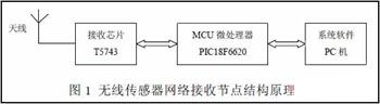
The wireless sensor network data receiving node module is mainly composed of the receiving chip T5743 and the MCU microprocessor PIC18F6620. Frequency and data transmission rate work together. The receiving chip T5743 communicates with the I / O port of the MCU microprocessor PIC18F6620 through the DATA serial bidirectional data line. When the MCU microprocessor receives data, it uses DATA_CLK as the synchronous clock. Special timing to achieve data reception and processing. The receiving process uses software control to carry out data transmission and realize the control of the receiving chip T5743. Before receiving data, the microprocessor PIC18F6620 writes the program in the MUC through the DATA line into the configuration register of the receiving chip, and performs Configure, and then wait for receiving data; when data comes, it is accessed by the LNA_IN terminal of the receiving chip T5743, amplified by a low-noise amplifier and sent to the mixer, so that it is transformed into an intermediate frequency; at the intermediate frequency level, the transformed signal is It is amplified and filtered before being sent to the demodulator.
Third, the receiving node chip
ATMEL's T5743 chip is an integrated UHF radio receiver module, a receiver chip with a PLL phase-locked loop structure, and is packaged in SO20. T5743 chip is developed to meet the requirements of low data rate and low cost RF data transmission system. Its data transmission speed is 1 ~ 10kB / s, and the encoding method is Manchester or dual phase method, which can be used in the receiving frequency range. ASK data transmission from 300MHz to 450MHz (433.92MHz and 315MHz); high sensitivity, fully integrated VCO, can realize low power consumption function, power supply voltage 4.5V ~ 5.5V; single-ended RF output is easy to print with antenna or PCB version The antenna is compatible; the working temperature range is -40 ℃ ~ 105 ℃.
The T5743 chip has a bidirectional serial data interface DATA, through which the DATA chip can communicate with the MCU serially and exchange information. It can work in two typical frequencies 433.92MHz and 315MHz, selected by the MODE pin, set high to 433.92MHz, set low to 315MHz, the receiving frequency is selectable between 1kB ~ 10kB, set by the software. The design uses a 1MHz intermediate frequency and a front-end SAW filter to achieve high image suppression. Based on the new SAW device, it achieves 40dB suppression, and can communicate with the microcontroller using a simple two-way data line, using a separate pin Power management is realized via the microcontroller.
The RF front end of the T5743 chip is a superheterodyne structure that converts the RF input signal into a 1MHz IF signal. The RF front-end consists of a low-noise amplifier LNA, a local oscillator LO, a mixer and an RF amplifier. LO is the carrier frequency generated by the PLL phase-locked loop and is used by the mixer. The RF signal is input through the RF input pin LNA-IN. At 433.92MHz, the input impedance is 1000Ω / pF. When designing the input network, first consider the noise matching, and adjust the component value and the printed circuit board's distributed inductance and capacitance to match the input terminal T5743 has the highest sensitivity at high signal-to-noise ratio. In this way, the signal from the RF front-end is filtered by a fully integrated 4th order IF filter to reach the application of 334.92MHz, and the center frequency of the intermediate frequency is l MHz.
The working mode of the demodulator in the design is set by the register OPMODE, the logic "L" sets the demodulator to FSK mode; the logic "H" sets the demodulator to ASK mode. In the ASK mode, an automatic threshold control circuit is used, which sets the detection reference voltage to an appropriate value that can obtain a good signal-to-noise ratio. This circuit can also effectively suppress any type of in-band noise signal or competitive emissions. If S / N The data signal can be detected well if it exceeds 10dB. In FSK mode, digital signals can be detected if S / N exceeds 2dB.
The output signal of the demodulator is filtered by a digital filter and sent to a digital signal processing circuit. The passband of the digital filter matches the characteristics of the data signal. The digital filter consists of a first-order high-pass and a third-order low-pass filter. The cut-off frequency fcu_DF of the high-pass filter is determined by formula (1). The cut-off frequency of the low-pass filter is determined by the selected baud rate range (BR-Range). BR-Range is set in the OPMODE register. The setting of BR-Range must be adapted to the baud rate.
All timings of the digital circuit and analog filter of the receiving node of the wireless sensor network come from a clock. This clock cycle TCLK is obtained from the crystal oscillator through the frequency divider, and the number of frequency divisions is controlled by the logic state at the MODE pin. The frequency of the crystal oscillator is determined by the RF input signal, which also determines the local oscillator frequency (fLO). The working state of the T5743 chip is set by two 15-bit RAM registers of OPMODE and LIMIT. The register can be programmed by the bidirectional DATA port. If the content of the register changes due to a power failure, this state is indicated by an output called a reset indicator (RM), in which case the receiving circuit must be reprogrammed. After power-on reset (POR), the register is set to the default mode. If the receiver works in the default mode, there is no need to program the register. Similarly, if the receiving circuit is not in the reset mode, the corresponding OFF command programming will be started; if the receiving circuit is in the reset mode, the corresponding OFF command programming will not be started, and the reset flag will still be displayed on the DATA pin.
Ejuice Recipe,Fruit-Flavored E-Cigarette Oil,Pure Ice Flavored Vape,Wholesale E Cigarette Vape
Shenzhen Niimoo Innovative Technology Co., Ltd , https://www.niimootech.com