In recent months, some major semiconductor manufacturers and IC foundries have announced the transistor size of micro ICs to 14 nanometers (nm), which reduces the size and cost of the Internet of Things (IoT) system single-chip (SoC). Paving in one step.
However, Tom Starnes, an analyst with semiconductor industry at ObjecTIve Analysis, said that it is not so fast in terms of development time. He pointed out that "most of the news released today is related to the standard microprocessor architecture, and has little to do with the requirements of IoT devices."
"These are mostly digital systems. It's not easy to really shrink to such a small geometry. It's easy to get close to the requirements of a microcontroller-based IoT device."
MCU-based SoCs are not just a combination of digital components, but also a large number of analog functions, wireless RF circuits, flash memory and static random access memory (SRAM) - none of which can be like a digital transistor It's as easy to shrink or predictable.
"There will be a viable MCU SoC market for the Internet of Things that will be able to take advantage of process nodes that are scaled down to 14nm to 20nm or less, but not now," Starnes said.
Sandeep Kumar, senior vice president of global operations at Silicon Labs, agrees. He also pointed out that the IoT SoC of the terminal node has different requirements and challenges than the fully digitized SoC.
"Wireless connectivity, integrated MPU, low-power operation, low-leakage SRAM and non-volatile memory (NVM) intellectual property rights (IP), all of which make process technology choices more critical." Kumar added: "Kumar added: " These IoT SoCs do not chase Moore's law in the same way that digital SoCs are commonly used."
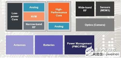
The MCU SoC in the wireless IoT endpoint combines a range of functions, including non-volatile memory and sensors, analog/mixed signals, narrowband wideband RF, and other peripheral functions such as antennas, batteries, and power management.
Kumar, based on the experience of Silicon Labs, is designed to target low-power consumption in consumer wearable devices, home automation, smart meters, smart lighting, health and fitness, factory automation, transportation, logistics and agriculture. , low data rate wireless connectivity applications. To support this type of design, Silicon Labs still manufactures ARM-based 32-bit wireless SoCs using a 90nm process. Kumar said that the company has not seen an urgent need to further advance the process node in the short term.
“The complex, energy-efficient radio frequency (RF) design for wireless connectivity, and the analog function for sensing or connecting low-voltage current sensors are just as critical as the digital performance of IoT SoCs,†Kumar said. SoC is not a key application for power consumption requirements such as desktop personal computers (PCs), mobile PCs, tablets or even mobile phones like IoT endpoints.
“IoT SoCs are used in wireless applications that often operate with button cells for 5-10 years. The low-leakage SRAM and high-tolerance NVM IP used in this technology node make it difficult to follow when designing these SoC products. Track the minimum process of Moore's Law."
According to Kumar, cost is another very important consideration when designing and manufacturing these SoCs.
When designing complex analog connectivity for IoT SoCs, the option to use NVM and mixed-signal RF technology has led to an increase in the number of wafer layers. It's really important to use a smaller process node to create an SoC that adds even more layers to make it more costly. In a design where the best cost/performance balance is the key to success, this is really important. Concerns.
“The IoT market is very fragmented and wide-ranging,†Kumar said. “The range of applications ranges from wearable devices, medical devices, automobiles, to industrial automation and agriculture. There are specific needs in every application area of ​​the Internet of Things. For some special applications, it is not necessarily because of the large market. And reduce costs."
Freescale Semiconductor faces similar pressures. While the company retains the ability to manufacture a wide range of proven products, Freescale has begun working closely with several key foundries as processes in some key product areas have shrunk to below 90 nm.

As semiconductor processes progress to the nanoscale, IC manufacturing will be driven by two conflicting requirements: high-performance digital ICs, and the mixed-signal requirements for MCU SoCs for a range of networking applications.
According to Ronald MarTIno, vice president of application processor business and advanced technology promotion at Freescale Semiconductor, the company still uses its in-house fab to develop its own design based on the foundry-based process. Once you have the combination of the various functions and power requirements you need, the final production will be handed over to the foundry. The company is currently moving its KeneTIs family of IoT MCUs to 40nm – this is its 28nm fully depleted over-insulated FD (FD-SOI) i.MX media processor and QorIQ network for its 16nm FinFET The next generation of technology for processors.
For MCU vendors in the IoT market, although cost and processor performance are important factors, power efficiency is more important in this design of terminal nodes powered by batteries or environmental energy.
“Although seemingly small process nodes will bring you low-power operation, the narrowing of the various components will make the road to the destination very rugged,†IHS Global Inc. Embedded Processor General analyst Tom Hackenberg said, "However, the gap is rapidly shrinking. Five years ago, some analog or RF components were about 3-4 process nodes behind digital components."
“Now, the gap has narrowed to 1-2 nodes, and we will soon see IoT device vendors using 32-bit MCUs turning to 28nm~50nm, depending on whether all components (such as Analogy applies, many of which still depend on the profit margin of their target market."
In fact, the winners of the Internet of Things are not the ones with the most powerful and advanced process node strategies, but those who know how to master various related technologies, applications and market needs, and have the expertise to know the timing of the most appropriate process. the company.
Weatherproof/Waterproof Type F Outlets
"Waterproof Type F Outlets Black,Waterproof Type F Outlets,Waterproof Outlet Plug,Waterproof Exterior Outlet "
Yang Guang Auli Electronic Appliances Co., Ltd. , https://www.ygpowerstrips.com