The so-called RF MEMS is an RF product processed by MEMS technology. RF-MEMS technology is expected to achieve high integration with MMIC, making it possible to create a system integrated chip (SOC) that integrates the collection, processing, transmission, processing and execution of information. According to the concept of microelectronics technology, not only wafer level production, product batching, but also cheap, small size, light weight, high reliability and so on. RF MEMS devices can be divided into two main categories: one is called passive MEMS, and its structure is free of movable parts; the other is called active MEMS, which has a movable structure. Under the action of electrical stress, the movable parts will Deformation or movement occurs. Its key processing technologies are divided into four categories: planar processing technology, bulk silicon etching technology, solid phase bonding technology, and LIGA technology.
RF MEMS is one of the important application areas of MEMS technology, and it is also a research hotspot in the MEMS field since the 1990s. RFMEMS are used in signal processing in RF and microwave frequency circuits and are a technology that will have a significant impact on the RF structure of existing radars and communications. With the advent of the information age, in the field of wireless communications, especially in the field of mobile communications and satellite communications, there is an urgent need for new devices with low power consumption, ultra-small planar structures that can be integrated with signal processing circuits, and hope that Covers broadband bands including microwaves, millimeter waves, and submillimeter waves. In the current communication system, there are still a large number of indispensable off-chip discrete components, such as inductors, variable capacitors, filters, couplers, phase shifters, switch arrays, etc., which become a bottleneck for further narrowing the system size. The emergence of RF MEMS technology is expected to solve this problem. Passive devices fabricated using RF MEMS technology can be integrated directly into the same chip with active circuits, enabling on-chip high integration of RF systems, eliminating parasitic losses caused by discrete components, and truly achieving high system cohesion and low Coupling can significantly improve the performance of the system.
First, the RF SOI process can operate at high frequencies, Ft/Fmax meets the requirements of 3 to 5 times the millimeter wave operating frequency; RF SOI can implement device stacking, thereby increasing power and energy efficiency ratio; again, RF SOI The substrate used in the process reduces parasitic effects, so that the fabricated RF chip has higher quality factor, lower loss, better noise figure, and the substrate also improves the insulation level and linearity of the product. Fourth, RF SOI can integrate logic and control functions, which is not possible with GaAs technology. Therefore, GaAs devices need to be combined with a control chip in the application. The RF and SOI process can be used to integrate PA and control functions on one chip. The cost is reduced while saving valuable PCB area; finally, the RF-SOI has a back-gate bias function, which can be used to fine-tune the millimeter-wave RF line to suit the needs of the application.
After reviewing the development of China's smart phone industry, Wang Qingyu, the general manager of Xinao Technology, pointed out that with the growth of the number of smart phones, the demand for RF-SOI has also increased rapidly, which is very difficult for China to develop RF-SOI. Opportunity, but there are also many challenges.
The RF device and manufacturing process market is heating up, especially for the two key components used in smartphones - RF switching devices and antenna tuners.
RF device manufacturers and their foundry partners continue to introduce traditional RF switch chips and tuners based on RF SOI process technology for today's 4G wireless networks. Recently, GlobalFoundries introduced the 45nm RF SOI process for future 5G networks. RF SOI is an RF version of silicon-on-insulator (SOI) technology that utilizes the high resistivity characteristics of the built-in isolation substrate.
To change the market landscape, Cavendish KineTIcs, a fabless IC design company, is introducing a new generation of RF products and antenna tuners based on alternative process RF MEMS.
RF switches and tuners are two key components in the RF front-end module of mobile phones. The RF front end integrates the system's transmit/receive functions, where the RF switch routes the wireless signal and the tuner helps match the antenna to any frequency band.
Even without considering the changes in RF equipment and process types, the challenges of today's RF market are daunting. Paul Dal Santo, President and CEO of Cavendish KineTIcs, said: "A few years ago, RF was a fairly simple design, but now things have changed a lot. First, your RF front-end must handle a very wide range. The frequency band extends from 600MHz to 3GHz. With the advent of more advanced 5G technology, the frequency band will be further extended to 5GHz to 60GHz. This brings some incredible challenges to front-end RF designers."
Mobile phone OEMs must face this challenge, make trade-offs, and consider new components. Specifically, for RF switches and antenna tuners, it can be attributed to two technologies - devices based on RF SOI processes and RF MEMS processes.
RF SOI is the manufacturing process currently in service. Devices based on the RF SOI process can meet current requirements, but they are beginning to encounter some technical problems. In addition, there are price pressures in the market, and some problems will arise as the device migrates from 200mm to 300mm.
In contrast, RF MEMS has some interesting features and has made progress in some areas. In fact, Cavendish KineTIcs said its MEMS antenna tuner based on RF MEMS technology is being used by Samsung and other OEMs.
Strategy AnalyTIcs analyst Chris Taylor said: "RF MEMS can provide very low on-resistance, which reduces insertion loss. But RF MEMS lacks production tracking records, and high-volume wireless system OEMs will not blindly focus on new technologies and small Vendors pay. Of course, RF MEMS prices must be competitive enough compared to RF SOI devices, but one major obstacle is that OEMs need to verify product reliability and require a reliable source of supply."
RF front endSmartphones are a big market for mixed RF switches, antenna tuners and other component business environments, and their data is worth a look. According to Pacific Crest Securities, global smartphone shipments are expected to grow by 1% in 2017, and in the past 2016, smartphones grew at an annual rate of only 1.3%.
On the other hand, according to YoleDéveloppement, the market size of the RF front-end module/component for smartphones is expected to jump from $10.1 billion in 2016 to $22.7 billion in 2022. According to Strategy Analytics, in 2016, the RF switch equipment market was $1.7 billion.
The RF market is growing as OEMs continue to add more RF components to their smartphones. "Multi-band LTE is also spreading to low-end devices," said Strategy Analytics' Taylor. “The RF switch component market is growing.â€
As the mobile network moves to 4G or Long Term Evolution (LTE), the number of RF switch devices per handset has increased. "The unit of shipment we are talking about is huge," Taylor said. “Now, most RF switching devices (not all) are used on mobile phones, most of which use RF SOI manufacturing processes. RF MEMS are still new and insignificant compared to RF SOI switches.â€
Despite the huge shipments of RF switches, the market is highly competitive and price pressures are high. According to Taylor, the average selling price (ASP) for these devices is 10 to 20 cents.
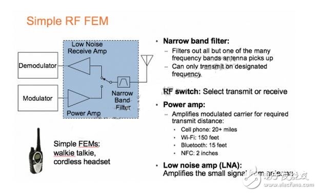
At the same time, in a simple system, the RF front end consists of multiple components - a power amplifier, a low noise amplifier (LNA), a filter, and an RF switch.
Randy Wolf, a GlobalFoundries technician, said in a recent speech: "The main purpose of a power amplifier is to ensure that there is enough energy to get your signal or information to the destination.
The LNA amplifies the small signal from the antenna. An RF switch routes signals from one component to another. "The filter prevents any unwanted signals from entering the back end," Wolf said.
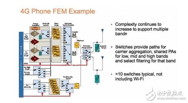
On mobile phones, the RF capabilities of 2G and 3G wireless networks are very simple. 2G has only four bands, and 3G has five bands. But 4G has more than 40 frequency bands. 4G not only combines the 2G and 3G frequency bands, but also carries a series of 4G frequency bands.
In addition, mobile operators have deployed a technology called carrier aggregation. Carrier aggregation combines multiple channels or component carriers into one big data pipeline to achieve higher bandwidth and faster data rates in wireless networks.
To address multiple frequency bands and carrier aggregation, OEMs need complex RF front-end modules. Today's RF front-end modules integrate two or more multimode multiband power amplifiers, as well as multiple switches and filters. “It depends on the RF architecture used. The number of power amplifiers is determined by the regional band that the handset can address.†Abhiroop Dutta, Qorvo Mobile Strategic Marketing Manager, said: “Using a single SKU to address multi-regional/global cellular markets globally Typical "full Netcom" mobile phones have a wide range of frequency coverage. In the implementation of the typical integrated RF front-end module of this mobile phone, one engineering option is to use a radio frequency front-end with a sub-band module to cope with the different requirements of high, medium and low frequency bands. ."
In contrast, there is another situation where smartphone OEMs may design dedicated handsets for specific markets. “An example is a mobile phone for the Chinese mainland market. In this case, the RF front-end needs to support the unique frequency bands in the region,†Dutta said.
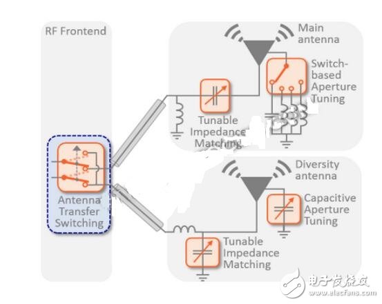
According to Cavendish Kinetics, there are two types of antennas, the main set antenna and the diversity antenna on the LTE handset. Basically, the main set antenna is used for transmitting/receiving functions, and the diversity antenna is used to increase the downlink data rate of the mobile phone.
In actual operation, the signal first arrives at the main set antenna and then moves to the antenna tuner, which allows the system to adjust to any frequency band. The signal then enters a series of RF switches. "It translates to the applicable frequency band you want to use, such as GSM, 3G or 4G," said GlobalFoundries' Wolf. "From there, the signal enters the filter, then the power amplifier, and finally reaches the receiver."
Given this complexity, handset OEMs face some challenges, and power consumption and size are critical. "Because of this complexity, the signal will suffer more losses at the front end, which will have a negative impact on the overall noise figure of your receiver," Wolf said.
Clearly, RF switches play a key role in solving this problem. In general, a smartphone may contain more than 10 RF switch devices. The basic RF switch is available in a single pole single throw (SPST) configuration. This is a simple on-off type switch.
Today, OEMs use more complex switch types. Ron * Coff is a key indicator of RF switches. According to Peregrine Semiconductor, "Ron * Coff reflects how much loss (Ron or on-resistance) occurs when the RF signal passes through a switch that is in the "on" state, and how much energy the RF signal leaks through the capacitor when the switch is in the "off" state ( The ratio of Coff or turn-off capacitor)."
All in all, OEMs need RF switches that have no insertion loss and good isolation. Insertion loss involves loss of signal power. If the RF switch does not achieve good isolation, the system may experience interference. “Overall, the challenge for RF front-ends is to support the growing performance demands and keep pace with evolving standards and increasing frequency band coverage. Not only that, but because of the thinning of handsets, the package size of RF solutions is also Zooming out. Qorvo's Dutta says key metrics such as insertion loss, antenna power and isolation are still driving the push for RF portfolio solutions.
solutionToday, mobile phone power amplifiers mainly use gallium arsenide (GaAs) technology. A few years ago, OEMs moved manufacturing processes such as RF switches from GaAs and sapphire (SoS) to RF SOI. GaAs and SoS are variants of SOI, and as RF switches become more complex, these two processes become too expensive.
RF SOI is different from fully depleted SOI (FD-SOI) and is suitable for digital applications. Similar to FD-SOI, RF SOI has a very thin insulating layer in the substrate, enabling high breakdown voltage and low leakage current.
Peter Rabbeni, head of RF business at GlobalFoundries, said: "The mobile market continues to be optimistic about RF SOI because it provides low insertion loss, low harmonics and high linearity over a wide frequency range, achieving good performance and cost efficiency."
Today, companies such as Qorvo, Peregrine, and Skyworks offer RF SOI-based RF switches. Typically, RF switch manufacturers use foundries to manufacture these products. GlobalFoundries, STMicroelectronics, TowerJazz and UMC are the leaders in the RF SOI foundry business.
As a result, OEMs have multiple options for component suppliers and foundry products. Typically, foundries offer RF SOI processes covering nodes from 180nm to 45nm and different wafer sizes.
Deciding which node to use depends on the specific application. Wu Kun, vice president of business management at UMC, said: "With regard to the specificization of RF SOI technology, everything is considering technical solutions for end applications from the perspective of technical performance, cost and power consumption."
Even with multiple options, RF switch manufacturers face some challenges. The RF switch itself contains a field effect transistor (FET). Like most devices, FETs are affected by unwanted channel resistance and capacitance.
In the RF switch, the FETs are stacked. In general, 10 to 14 FETs are stacked in today's RF switches. According to experts, as the number of FETs increases, devices may experience problems associated with insertion loss and resistance.
Another issue is the capacitor. In an article published in 2014 entitled "The Latest Developments and Future Trends in SOI Processes in RF Applications," Skyworks said, "In RF switches, 30% or more of the unwanted capacitors come from interconnects in the device. The interconnect is a metal layer or micro-wiring scheme that includes RF SOI-based switches.
Typically, in 4G handsets, the mainstream manufacturing process for RF switches is the 180nm and 130nm nodes of a 200mm wafer. Many, but not all, interconnect layers are based on aluminum. Aluminum interconnects have been used in the IC industry for many years and are inexpensive, but also have higher capacitance.
Therefore, copper is used for some selected layers in RF devices. Copper is a better conductor and has a lower electrical resistance than aluminum. Ng said: "The traditional metal stack for 130nm RF CMOS process products includes a cost-effective aluminum interconnect layer and a copper interconnect layer with performance advantages." This is the best solution for balancing cost and performance. RF SOI solutions typically contain a certain number of aluminum metal layers and one or more copper layers.
Typically, copper is used as an ultra-thick metal layer on the top layer to help improve passive device performance. He said: "It is best to have a thick top layer of copper, which minimizes ohmic losses and improves performance."
Recently, RF equipment manufacturers have migrated from 200mm wafers to 300mm wafers, and their process nodes have also migrated from 130nm to 45nm. Typically, 300mm fabs use only copper interconnects.
Using only copper interconnects, RF switch manufacturers can reduce capacitance. However, 300mm wafers increase manufacturing costs and create some contradictions in the market. On the one hand, cost-sensitive handset OEMs need RF switches to keep prices low. On the other hand, RF switchgear manufacturers and foundries hope to keep profits.
“Today, only a few RF SOI devices are produced on 300mm wafers,†Ng said. “There are many reasons for this, including the cost/availability of 300mm RF SOI substrates and the infrastructure to support post-silicon processing. However, we expect these challenges to be significant in the next few years. The solution is resolved, and then most of the high-volume RF SOI applications will migrate to 300mm wafers."
Prior to this, the industry may face 300mm supply and demand issues. “We believe that the market will continue to face the challenge of being in short supply before more production migrates to 300mm wafers. How fast the production capacity will be and how much demand will be reflected in the contradiction between supply and demand,†he said.
Today's RF SOI process is suitable for 4G mobile phones. GlobalFoundries hopes to stand out in the 5G competition and recently launched the 45nm RF SOI process for 5G applications. This process utilizes a high resistance well enriched SOI substrate.
5G is an upgrade of 4G networks. Today's LTE network bands range from 700 MHz to 3.5 GHz. In contrast, 5G not only coexists with LTE, but will also operate in the millimeter band between 30 GHz and 300 GHz. 5G increases the data transmission rate to more than 10 Gbps, which is 100 times that of LTE. But the large-scale deployment of 5G is expected to be in 2020 and beyond.
In any case, 5G needs a new component. "(45nm RF SOI) is mainly focused on the 5G millimeter wave front end, which integrates PA, LNA, switches, phase shifters, and creates an integrated millimeter wave controllable beamformer for 5G systems," said Rabbeni of GlobalFoundries.
There are other solutions for 5G, and RF MEMS is one of them. In addition, TowerJazz and the University of California, San Diego, recently demonstrated a 12Gbps 5G phased array chipset. The chipset uses TowerJazz's SiGe BiCMOS technology.
Which process will win? Only time will tell us the answer. "It is not clear whether RF MEMS has an advantage in 5G applications," said Strategy Analytics' Taylor.
What is RF MEMS?RF SOI-based RF switches will continue to dominate, but new technologies RF MEMS may also have some room for survival. "Over time, SOI has made incredible progress. Resistance has dropped and linearity has improved," said Dal Santo of Cavendish Kinetics. "But the essence of a SOI switch is that a transistor turns on or off. When turned on, it does not perform very well. When turned off, it is not very good.
RF MEMS technology has been moving steadily for many years. Today, Cavendish, Menlo Micro and WiSpry (AAC Technologies) are developing RF MEMS for mobile applications.
RF MEMS are different from sensor-based MEMS such as gyroscopes and accelerometers. Sensor MEMS converts mechanical energy into electrical signals. In contrast, RF MEMS only conduct signal conduction.
Initially, companies such as Cavendish applied RF MEMS technology to the antenna tuner market using RF SOI and other processes.
"If the antenna is fixed, we can't make it support the different frequency bands needed. So the antenna needs to be adjusted," Dal Santo said. "Now, the main method is to switch, either switching between different fixed capacitors or switching different fixed inductors. The problem is that the antenna is a high-Q device. You must be careful, otherwise it will cause loss of radiation performance."
In contrast, Cavendish's tuner has 32 different capacitance ranges. “They are fully programmable and have very good high Q performance. So the loss of radiated performance is very low. You can use these to adjust the antenna to the frequency range you need to support,†he said.
Looking ahead, Cavendish plans to use RF SOI devices in the larger RF switch field. He said: "If you replace the RF SOI with a real switch, that is the MEMS switch, the insertion loss of your receiver or transmitter will be reduced," he said.
But will RF MEMS devices replace RF SOI-based devices? TowerJazz can provide some insight into this issue. TowerJazz offers a traditional RF SOI process and is a foundry of Cavendish's RF MEMS devices.
“RF MEMS and RF SOI may have some small overlap in competing applications. In general, they complement each other, RF MEMS is used for the most demanding applications, and RF SOI is used for the rest of the application, “TowerJazz Marco Racanelli, senior vice president and general manager of the RF / High Performance Analog Business Unit, said.
"RF SOI technology will continue to evolve, and it is still available for RF switching applications and some low noise amplifier markets," Racanelli said. “However, in some special applications, alternative technologies such as SiGe for low noise amplifiers and MEMS for switching can provide better linearity or lower losses. In short, RF SOI will continue to be an expanding market. Services, other technologies will also develop."
RF MEMS has already taken a place in the antenna tuner market, and it will take time to verify whether it can extend the antenna to the RF switch business. "In the future, RF MEMS can help increase the data rate of mobile phones by providing more linear and lower loss switches than built-in RF SOI," he said. “In RF MEMS, metal plates can be in direct contact in a “on†state, forming a metal, low loss, linear connection. Higher linearity allows for more frequency bands and more complex modulation schemes, thereby increasing the handset’s Data rate.
Copper Flat Wire Rolling Machine
Copper Flat Wire Rolling Machine,Special Shaped Copper Strip Machine,Ultra Thin Copper Strip Machine,Copper Strip Annealing Equipment
Jiangsu Lanhui Intelligent Equipment Technology Co., Ltd , https://www.lanhuisolar.com