As a general-purpose power supply, switching power supply is known for its light, thin, small and high efficiency. It is an indispensable power supply method for miniaturization and low cost of various electronic devices, and has become the mainstream power supply of today. . With the rapid development of the electronic information industry, its application range will also be expanded, and the demand will increase day by day. However, when people enjoy the convenience of light, thin, small, and high efficiency brought by the switching power supply, they also bring various kinds of noise interference. In particular, the switching power supply is developing toward a smaller volume, higher frequency, and higher power, and the EMI noise caused by dV/dt and dI/dt will be larger. Its conducted noise and radiated noise will affect the safety of the whole machine, sometimes it will interfere with some CPU commands, causing misoperation of the system, and in serious cases, it will cause subversive damage to the system. To this end, we should pay close attention to the harm caused by the EMI noise of the switching power supply when using the switching power supply, and take active precautions to reduce EMI noise and minimize the impact of EMI noise.
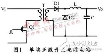
1 EMI noise currentSwitching power supply has many circuit topologies. According to the combination of power switching tube and high frequency transformer, it can be divided into full bridge, half bridge, push-pull, single-ended forward, single-ended flyback and other modes. In the small and medium power switching power supply modules, more circuit topologies are used as push-pull, single-ended forward, single-ended flyback, and the like. A typical single-ended forward switching power supply circuit block diagram is shown in Figure 1. It consists of a power switch tube Q1, a high-frequency transformer T, a rectifier diode Dl, a freewheeling diode D2, an output filter inductor L, and an output filter capacitor C. During operation, the PWM control unit can send a pulse signal with variable pulse width to drive the switch tube Q1. When the switch tube Q1 is turned on, the DC energy of the input end is transmitted to the secondary through the high-frequency transformer, and when the switch tube Q1 is turned off, The high frequency transformer is magnetically reset. The high-frequency pulse transmitted through the high-frequency transformer is rectified by the rectifier diode into a single-direction pulsed DC. This pulsed DC is filtered by the output filter inductor and the filter capacitor, and the required DC voltage can be sent.
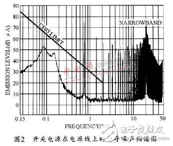
During the switching of the high frequency switch of the power switch tube Q1, the pulses flowing through the power switch tube and the high frequency transformer generate a complicated harmonic voltage and harmonic current. The noise generated by these harmonic voltages and harmonic currents can be transmitted to the common power supply through the power input line or to the load through the output line of the switching power supply, thereby causing interference to other systems or sensitive components. The noise spectrum of these noises transmitted on the power line is shown in Figure 2. It can be seen from the figure that in the frequency band of several hundred kHz to 50 MHz, that is, the fundamental wave of the switching frequency and the frequency band of several harmonics. Within, the amplitude of the interference noise far exceeds the range specified by GJBl51A, and thus the electromagnetic compatibility index such as system conduction noise will exceed the standard.
Then how is this noise formed, and how does it spread? The following is an example of a surface-mounted switching power supply module with a medium- and small-power metal package structure.
1.1 Common mode interference current
The entire circuit components of the metal package structure surface mount switching power supply module are all mounted on the substrate. Active devices such as PWM control chips, power switch tubes, and rectifier diodes all use surface mount package components. The input and output voltage and current are sent out by the lead, and its internal structure is shown in Figure 3.
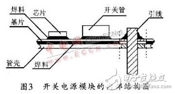
The bottom plate of the shell is the carrier of the alumina substrate, the front side of the alumina substrate is the wiring area and the assembly area of ​​the components, the back side is metallized with a thick film paste, and then passed through the solder (such as solder) and the tube case. The metal base plate is connected. The alumina substrate has a dielectric constant of 8, and the thickness is usually in the range of 0.5 to 1.0 mm. In the assembly area on the front side of the alumina substrate, surface mount components (such as PWM control chip, op amp, reference source, MOSFET switch, rectifier diode) pass through solder (such as conductive paste, reflow solder, etc.) and wiring The pads of the zone are connected. Although such a connection method constitutes a circuit loop, it also brings a new parasitic capacitance Cp to the circuit. The distribution of these parasitic capacitances is shown in Figure 4.
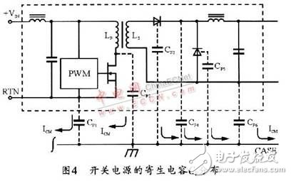
In the primary loop, the power switch transistor chip, the PWM control chip, the operational amplifier chip, the trace of the positive and negative input lines of the power supply, etc., and the parasitic capacitance Cp are generated between the substrate and the bottom plate of the casing. The size of the parasitic capacitance depends on the thickness of the substrate. And the area they occupy on the bottom plate. Thus, in the circuit, distributed capacitances Cp1, Cp2, ..., Cp6, etc. are formed between these components and their traces and the bottom plate of the casing. These distributed capacitances cause noise currents under the combined influence of dV/dt, dI/dt, and reverse recovery current of the rectifier diode. These noise currents are equal in magnitude and phase between the positive and negative of the input power line and the positive and negative of the output load line, which is called common mode noise current. The magnitude of the common mode noise current is related to the size of the distributed capacitance, dV/dt, dI/dt, and so on.
1.2 Primary differential mode interference current
Figure 5 shows a schematic diagram of the primary differential mode interference current. In the primary circuit, the power switch tube Q1, the high-frequency transformer primary winding Lp and the input filter capacitor Ci constitute an input DC conversion loop of the switching power supply, and this conversion loop passes the input DC energy through the high-frequency transformer during normal operation. Pass to the secondary. However, when the power switch Q1 is switched, the fundamental wave and harmonics caused by the rising and falling of the high-frequency pulse are transmitted along the input filter capacitor Ci to the input power supply terminal. This noise current propagates along the positive and negative ends of the input power line. It is called the primary differential mode interference current IDIFF.
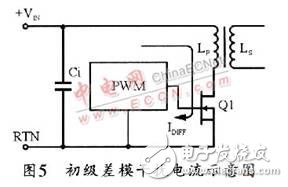
The differential mode interference current IDIFF flows to the common power supply terminal through the input power line, especially when the input filter capacitor Ci is insufficiently filtered, the interference to the input power line is large, and it also interferes with other parts of the system through the common power supply terminal. Thereby the performance index of other parts is lowered.
1.3 Secondary differential mode interference current
Luxry Lift,Home Elevators,Luxry Home Lift,Elevator For Home Use
XI'AN TYPICAL ELEVATOR CO., LTD , https://www.chinaxiantypical.com