Designed and implemented FPGA-based programmable digital downconverter (DDC) for wideband digital intermediate frequency software radio receivers, mainly for digital down conversion, data extraction and other functions. The top-down modular design method is used to divide the entire downconverter into basic units to implement these functional modules and form a module library. In specific applications, each module is optimally configured to meet the performance requirements of a particular wireless communication system.
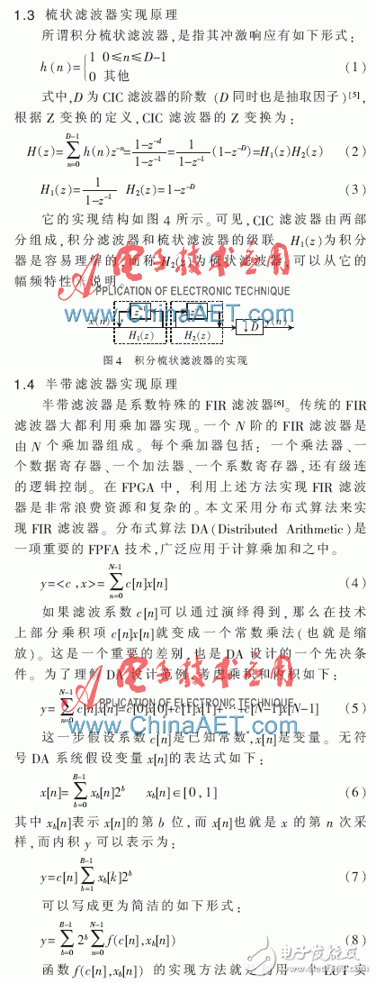
Digital down conversion technology has important application value in the fields of mobile communication, digital broadcasting, and television. In the receiver, the signal is mixed and output to a low-pass filter to filter out the multiplier component and the out-of-band signal. However, with the increase of sampling rate, an important problem is that the data stream rate after sampling is very high, which leads to the subsequent signal processing speed can not keep up, especially for some synchronous demodulation algorithms, the computational amount is huge [1]. Too high data throughput is difficult to meet real-time requirements, so it is necessary to slow down the A/D converted data stream.
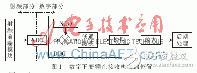
The basic function of digital downconversion is to extract the required narrowband signal from the input wideband high speed data stream signal, downconvert it to a digital baseband signal, and convert it to a lower data stream [2]. The output signal of the high-speed ADC is sent to the digital down converter, and then mixed with the digital local oscillator, and then filtered by the bandpass filter to filter out other interference signals, and then the signal is demodulated and decoded. If the band-pass filtering is directly performed on the mixed data, the computational complexity is particularly large. For example, if the digital sampling rate of the signal is 30.72 MHz and the filter is a 33-order FIR filter, the filtering operation requires 1 013 M multiplications and 980 M additions, conventional DSP is unbearable. Therefore, the mixed signal must be decelerated, which is the main work done by the down converter, as shown in Figure 1.
1.1 System principle realization
The subsequent processing of the digital downconverter output signal is mainly to complete signal demodulation, decoding, anti-interference, adaptive equalization and signal parameter estimation [3]. Since the orthogonally decomposed I/Q two-baseband signals usually bring great convenience and good performance to the above-mentioned subsequent processing, the design adopts a typical structure of orthogonal two-way processing. Figure 2 is a block diagram of the design of the present design. Mainly include: numerically controlled oscillator, mixer, improved cascaded comb (MCIC) filter, half-band (HB) filter, decimator, programmable FIR filter, control module.
The analog IF signal is sampled by the analog-to-digital converter at the front end to obtain a digital intermediate frequency signal. The digital signal is first mixed with the two orthogonal local oscillator signals generated by the numerical control local oscillator, and the digital intermediate frequency is moved to the baseband. Since the ADC samples at the intermediate frequency, the sampling rate is likely to be high, and the data rate and sampling rate obtained after mixing are consistent. If the FIR filter is used directly, this processing rate cannot be achieved at all. Therefore, the mixed signal first passes through the CIC filter and the HB filter, and then is extracted to reduce the data rate, and then filtered by the FIR filter. Since the coefficients of the CIC filter are all 1, the implementation is very simple. Only the addition and subtraction operations can achieve a higher processing rate when implemented in hardware, which is suitable for the first stage in the extraction system and performs large multiple extraction. However, the characteristics of the CIC filter's stopband attenuation are not very good. It is usually necessary to increase the stopband attenuation by using a five-stage CIC filter cascade, with a decimation factor of 2-16. Since the in-band flatness of the CIC filter is not very good, a compensator is added to its back end, collectively referred to as a modified CIC (MCIC) filter. The HB filter is used as a second-stage low-pass filter because its coefficient is almost half zero and the amount of calculation during filtering is reduced by half. The decimation factor of the signal processed by the HB filter is fixed at 2, which is especially suitable for the requirement of reducing the sampling rate by half. After filtering by the MCIC filter and the HB filter, the baseband signal is reduced to a lower rate from the initial high data rate and is suitable for post-stage FIR filter processing.
1.2 Numerical control oscillator implementation principle
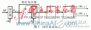
The numerically controlled oscillator is the generating mechanism of the local frequency oscillation signal. Its function is mainly to generate an ideal sine and cosine sequence with an oscillating frequency of intermediate frequency [4]. It is one of the most important factors determining system performance. The numerically controlled oscillator of this paper is realized by direct digital frequency synthesis technology.
Direct Digital Frequency Synthesis (DDS) is a new frequency synthesis technique that directly synthesizes the desired waveform from the phase concept. In recent years, the level of technology and devices has been continuously developed, which has led to the rapid development of DDS technology. It has completed a leap in frequency synthesis technology and is the most widely used frequency synthesis technology. The basic structure of DDS is shown in Figure 3.

1.5 Programmable FIR Shaping Filter Implementation Principle
In the multi-stage high efficiency digital filter module of the digital down converter, the final stage generally uses a programmable FIR filter to filter the entire channel. After the signal is filtered and filtered by the MCIC filter and the half-band filter of the previous stage, the sampling rate input to the FIR filter is relatively low, so the order of the filter can be appropriately increased under the premise of real-time processing. . Higher-order FIR filters can make the filter's passband fluctuation, transition bandwidth, and stopband attenuation better than [7].
The FIR filter is designed to pass the desired signal as much as possible while suppressing unwanted signals as much as possible. For the amplitude-frequency characteristics of the filter, the passband ripple is as small as possible, the passband width is as close as possible to the useful signal bandwidth, the transition band is as narrow as possible, and the stopband attenuation is as large as possible. The programmable FIR filter designed in this paper is realized by directly calling the IP core, and the order is 64 steps. It is still implemented by a combination of serial and parallel.
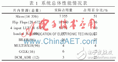
2 system verificationThe FPGA chip selected for this design is the Virtex II3000 from XILINX. The utilization of chip resources is shown in Table 1.
Select the input signal as x=cos(2Ï€(fc+f1)t+0.003 2cos2Ï€(fc+f0)t), where f1=0.3 MHz, f0=0.2 MHz, fc=30 MHz, and the selected sampling frequency is fs=80 MHz, decimation coefficient CW1=4, CW2=4, CW3=1, that is, the first-stage CIC filter performs 5 times extraction, the second-stage CIC filter performs 5 times extraction, and the whole system performs 100-times extraction, double The amplitude spectrum of the path output complex signal is shown in Figure 6. It can be seen from the spectrogram that the dynamic range of the digital downconverter is greater than 50 dB.
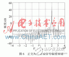
The main content of this paper is the design of digital down converter based on FPGA. Firstly, according to the objective requirements and the total available resources, the overall design scheme of the digital down converter is demonstrated. Then, the whole design is modularized according to the design scheme, and the design of each module is completed by adopting the idea of ​​top-down modular design. By configuring each of the decimated pins, 8~1 024 times of extraction can be achieved. Finally, the sinusoidal signal is used as the test signal, and the maximum dynamic range of the system is measured to be greater than 50 dB.
We provide many kinds of Polymeric Diaphragm to meet the different needs of different customers, they are widely used in Hi-Fi speakers,professional audio,horn speakers,car speakers and other high-end products.
We are experienced in manufacturing and have strong capability.
Our products are popular in many countries and areas.
We have professional acoustical testing systems and instruments.
We promise to offer you highest quality and best service!
Polymeric Diaphragm,Voice Coil Diaphragm,Diaphragm Voice Coil For Horn Driver,Voice Coil Phenolic Diaphragm
Taixing Minsheng Electronic Co.,Ltd. , https://www.ms-speakers.com