Aiming at the shortcomings of the traditional FIR filter, a design method of FIR filter based on FPGA multiplier is introduced. The filter uses the FPGA's own 18-bit multiplier MULT18 &TImes; 18SIO for multiplication calculation, using register pair multiplication results. The accumulation is performed to implement the FIR filtering function. The filter has the advantages of taking up very little resources, increasing the filtering speed and high speed flexibility.
In the fields of engineering systems such as communication systems, aerospace systems, radar systems, and remote sensing telemetry systems, filtering techniques are indispensable for both signal acquisition and transmission, and signal processing and conversion. Since the FIR filter has a strict linear phase and stability in the system, the FIR filtering technique has a wide range of applications [1-4].
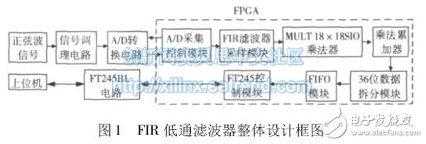
1 FIR low pass filter overall designThis article mainly introduces the FIR low-pass filter, which is mainly composed of hardware circuits and FPGA programs. The FIR filter hardware circuit is mainly composed of signal conditioning circuit, AD conversion circuit, FPGA control circuit, FT245RL circuit and host computer. The FPGA internal program module includes AD acquisition control module, FIR filter sampling module, MULT 18 &TImes; 18SIO multiplier Module, accumulation module, 36-bit data splitting module, FIFO module and FT245 control module. The main function of the filter is to use the signal generator to generate a sine wave of a specific frequency. After conditioning by the signal conditioning circuit, the 12-bit AD converter converts and outputs the digital signal. The FIR filter sampling module operates in a 60 MHz clock. And the digital signal outputted by the AD is sampled at a sampling rate of 10 kHz. The sampled digital signal value is output to the 18-bit multiplier module together with the FIR filter coefficient, and is multiplied and accumulated, and 36-bit data is accumulated. The USB interface composed of FT245 is transmitted to the host computer for curve display, and the obtained result is the filtered data. The system composition principle is shown in Figure 1.
2. 1 AD converter circuit
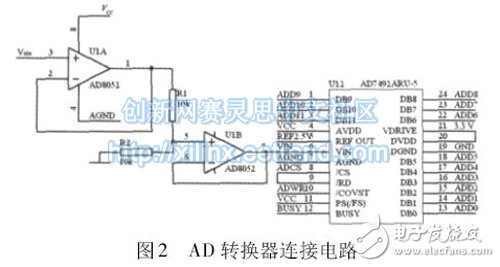
In this system, the sampling rate of the input voltage is 10 kHz, so the high-performance successive approximation A/D conversion chip AD7492BRU-5 of AD company is used, and the maximum conversion rate is 1.25 &TImes; 10 times/s with 12 bits. Parallel data output interface, and has a three-state function to meet system sampling requirements.
Since the reference voltage of the AD7492BRU-5 is 2.5 V, and the input analog signal range is 0 to 5 V, the signal needs to be properly conditioned before the analog signal enters the AD converter. The conditioning circuit is shown in Figure 2. . The output analog signal is divided by two 10 kΩ resistors to meet the input requirements of the A/D converter and output through the voltage follower without distortion.
2. 2 FT245 interface circuit
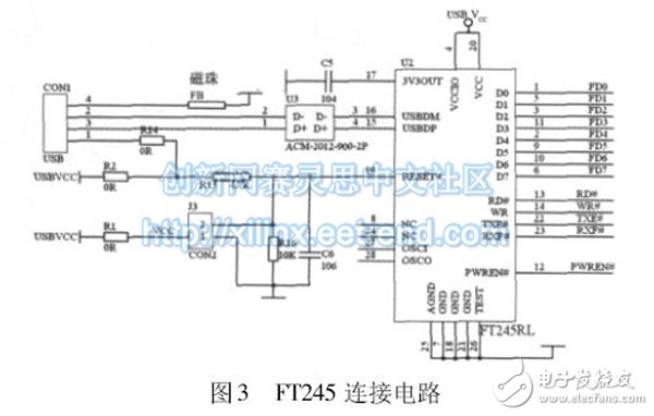
The filtered data sent by the FPGA in this system is transmitted back to the host computer through the USB interface, and the host computer reads the USB data and saves the data. The USB interface circuit uses FTDI FT245RL as the USB interface chip to realize data communication between the host computer and the FPGA. The FT245RL does not require a firmware program, can use the drivers provided by FTDI, and is compatible with the USB1.1 and USB2.0 protocols. The USB connection circuit is shown in Figure 3. The data transmission line of this circuit is connected to a common mode inductor ACM-2012-900. When there is common mode interference on the differential signals USBDM and USBDP, the magnetic field is superimposed due to the common mode signal. A high impedance is formed on the inductor to achieve the purpose of filtering out common mode interference. The USB port is grounded to a magnetic bead so that the connection can better prevent the power supply from being disturbed by data transmission. The USB interface reads data from the FPGA. Once the FPGA internally determines that a half full signal is generated in the FIFO, the data is transferred to the USB interface and finally read by the host computer.
This design uses the Xilinx XC3S400 FPGA for program verification. The XC3S400 is a high-density programmable logic device. The main features include a minimum of 5 ns of pin-to-pin logic delay, a global clock maximum pin maximum input frequency of 66 MHz, a core supply of 1.2 V, and an I/O port that can be set to 3. 3 V work. The device has a wealth of logic resources, including 16 MULT18 & TImes; 18SIO, which can perform a large number of multiplication operations [8].
The FIR filter program is mainly composed of a sampling module, a multiplier module, an accumulation and a module. The sampling module functions to acquire 60 sample values ​​and output the filter coefficients to the multiplier to multiply the sampled values. The main function of the multiplier module is to multiply 60 sample values ​​and 60 filter coefficients, and the resulting multiplication result is input to the accumulator. The accumulator is to accumulate the 60 results of the input to obtain the 36-bit filtering result [9-10].
3. 1 sampling module
The sampling module mainly samples the output value after AD conversion. In this design, the sampling rate is 10 kHz, that is, the sampling rate of AD is 10 kHz, and the sampling rate of the output value of the filter after AD conversion is also 10 kHz. Their implementation is procedurally synchronized. In the AD output module, each time the data conversion is completed, a rdy rising edge signal is generated. The sampling module receives and discriminates the rdy rising edge signal, receives the first data, and outputs the first filter coefficient to MULT18 × 18SIO. The multiplier simultaneously generates a rising edge signal to the CLK terminal of the multiplier, starts the multiplier to multiply, and the multiplication result is extremely short, so that high-speed multiplication can be realized.
Shenzhen E-wisdom Network Technology Co., Ltd. , https://www.healthy-cigarettes.com