There are many reasons for EMI in the PCB, such as: RF current, common mode, ground loop, impedance mismatch, magnetic flux, etc. In order to master EMI, we need to gradually understand these reasons and their impact. Although we can learn the mathematical basis of EMI phenomenon directly from electromagnetic theory, it is a very hard and long road. For the average engineer, a simple and clear description is even more important. This article will explore the "source of electricity" on the PCB, the application of the Maxwell equation, and the concept of magnetic flux minimization.
Source of electricityIn contrast to magnetic sources, the source of electricity is modeled by time-varying electric dipoles. This means that there are two separate, oppositely opposite, time varying point charges that are adjacent to each other. Both ends of the bipolar contain changes in charge. This change in charge is caused by the constant flow of current over the entire length of the bipolar. The oscillator output signal is used to drive an unterminated antenna that can be used to represent the source of electricity. However, this circuit cannot be explained by the low frequency circuit principle. Regardless of the limited propagation speed of the signal in this circuit (this is based on the dielectric constant of the non-magnetic material), the RF current will be generated in this circuit. This is because the speed of propagation is limited, not unlimited. The assumption is that the wire contains the same voltage at all points, and the circuit is balanced at any point. The electromagnetic field generated by this source of electricity is a function of four variables:
1. Current amplitude in the loop: The electromagnetic field is proportional to the amount of current flowing in the dipole.
2. The polarity of the bipolar and the relationship of the measuring device: as with the magnetic source, the polarity of the bipolar must be the same as the polarity of the antenna of the measuring device.
3. Size of the bipolar: The electromagnetic field is proportional to the length of the current component, however, the length of the trace must be only large for the wavelength portion. The larger the dipole, the lower the frequency measured at the antenna end. This antenna will resonate at a specific frequency for a particular size.
4. Distance: The electric and magnetic fields are related to each other. The strength of both is proportional to the distance. In the far field, the behavior is similar to the loop source (source of magnetism), and an electromagnetic plane wave appears. When approaching a "point source," the dependence of the electric and magnetic fields on the distance increases.
The relationship between the near field (the component of magnetism and electricity) and the far field is shown in Figure 1. All waves are a combination of magnetic and electric field components. This combination is called "PoynTIng Vector". In fact, there is no single radio wave or magnetic wave. The reason why we can measure the plane wave is because for a small antenna, the wavefront looks like a plane at a few wavelengths from the source.
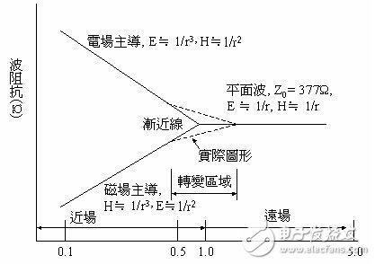
Figure 1: Relationship between wave impedance and distance
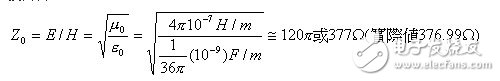
This appearance is the physical "contour" observed by the antenna; it is like floating from the river to the river. The water waves we see are a wave of ripples. Field propagation is a point source from the field, radiating outward at the speed of light; among them. The unit of measurement of the electric field component is V/m, and the unit of measurement of the magnetic field component is A/m. The ratio of the electric field (E) to the magnetic field (H) is the impedance of the free space. It must be emphasized here that in a plane wave, the wave impedance Z0, or the characteristic impedance called free space, is independent of the distance and is independent of the characteristics of the point source. For a plane wave in free space:
The energy unit carried by the wavefront is watts/m2.
For most applications of the Maxwell equation, the noise coupling method can represent a model of an equivalent component. For example, a time-varying electric field between two conductors can represent a capacitor. Between the same two conductors, a time-varying magnetic field can represent a mutual inductance. Figure 2 shows these two noise coupling mechanisms.
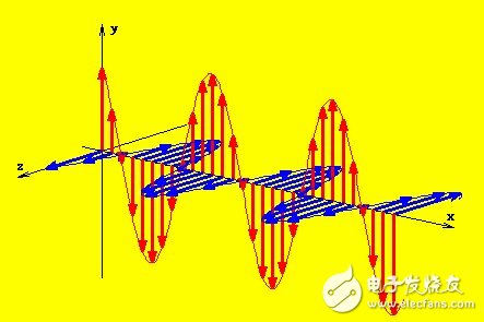
Figure 2: Noise coupling mechanism
Plane wave shape
For this noise coupling method to be correct, the actual size of the circuit must be smaller than the wavelength of the signal. If this model is not really correct, you can still use the lumped component to illustrate EMC for the following reasons:
1. Maxwell's equations cannot be directly applied to most real-world situations due to complex boundary conditions. If we don't have confidence in the approximate correctness of the lumped model, then this model is not correct. However, most of the lumped components (or discrete components) are reliable.
2. The numerical model does not show how noise is generated based on system parameters. Even if a model is probably the answer, system-related parameters are not predicted, identified, and visualized. Among all the available models, the model built by the lumped components is the best.
Why is this theory and discussion of Maxwell's equation important for PCB design and layout? The answer is simple. We must first know how the electromagnetic field is generated, and then we can reduce the electromagnetic field generated by the radio frequency in the PCB. This is related to reducing the RF current in the circuit. This RF current is directly related to the signal distribution network, bypass, and coupling. The RF current will eventually form harmonics of the frequency and other digital signals. The signal distribution network must be as small as possible to minimize the loop area of ​​the RF return current. Bypass and coupling are related to the maximum current and must be generated through the power distribution network to generate large currents; while the power distribution network, by definition, has a large loop area of ​​RF return current.
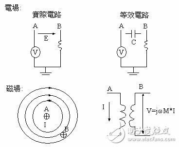
Figure 3: Noise coupling method
Face Plate,electrical face plates,cat6 faceplate,face plates
NINGBO UONICORE ELECTRONICS CO., LTD , https://www.uonicore.com