Recently, a research team led by Dr. Nanfang Yu, an assistant professor of applied physics at Columbia University, successfully used nano-antennas to invent a way to efficiently control light propagation in narrow paths, or so-called "waveguides". New way. The paper was published in the April 17 issue of Nature Nanotechnology.

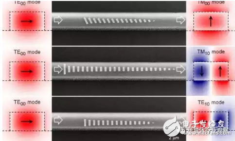
Figure|虞å—
Photonic integrated circuits (ICs) utilize light propagating in a waveguide for data transmission compared to integrated circuits that rely on electronics for data transmission. The key to creating such a circuit is to effectively control the process of light propagation. Professor Yan's method will bring people faster, more powerful and more efficient photonic chips. Not only that, but such chips will in turn bring about dramatic changes in photonic communication and photonic signal processing.
Professor Yan said that the integrated nanophotonic device we built is the smallest in history, but it has the widest working bandwidth to date. With the help of nano-antennas, we are able to greatly reduce the size of photonic integrated devices. The size reduction is no less than the big leap of replacing large vacuum tubes with semiconductor transistors in the 1950s. How can I control the light propagating in the waveguide in an efficient way? This issue has been the most fundamental and important scientific issue in this field. And our work has found a revolutionary answer to this problem.

The optical power of the light waves propagating along the waveguide is limited to the core of the waveguide: researchers can only find clues about the guided waves through the subtle, fading "tails" that exist near the surface of the waveguide. These unpredictable guided waves are particularly difficult to achieve precise manipulation. Therefore, in the past practice, photonic integrated devices are often designed to be larger in size, occupying space, and limiting the device integration density of the chip. Reducing the size of photonic integrated devices has been one of the challenges that researchers hope to overcome.
Professor Yu's team found that the most effective control for light propagating in a waveguide is to use a light nano-antenna to "modify" the waveguide. These miniature antennas are capable of absorbing light from inside the waveguide chip, changing the properties of the light, and then releasing the modified light back into the waveguide. The densely stacked nano-antennas exhibit a very strong cumulative effect, enabling them to perform functions such as waveguide mode conversion over a propagation distance of no more than two wavelengths.
Professor Yan said, “In traditional methods, the length of the devices we use is mostly hundreds of times the wavelength. With this in mind, our research is a major breakthrough. We have been able to reduce the size of the device. To the original tenth or even one percent."

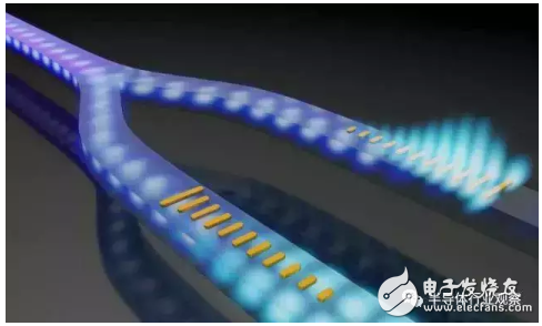
Figure | Schematic diagram of a photonic integrated circuit, in which one branch converts the incident basic waveguide mode into a second-order mode
The team of professors has created a mode converter that converts one waveguide mode to another. This converter is the key to the so-called "mode division multiplexing" (MDM) technology. An optical waveguide can carry a set of fundamental waveguide modes, as well as a series of higher order waveguide modes, just as the same guitar string can play both a basic sound and a part of a chord.
MDM can greatly enhance the information processing capability of an optical chip. Specifically, in the same waveguide, one can use multiple colors of light but different waveguide modes to simultaneously transmit multiple independent channels. For example, the effect is like the traffic carrying capacity of the Golden Gate Bridge has been expanded several times overnight. Professor Yan explained that our waveguide mode converter makes it possible to create more information channels.
Professor Yan's next step is to place the optical material with active adjustment into the photon integration period to achieve active control of the light propagating inside the waveguide. The device is expected to become a basic component of realistic enhancement (AR) glasses. The principle of realistic enhanced glasses is to first determine the wearer's spectacles aberrations and then project the corrected image into the spectacles.
Currently, Professor Yan is working with his colleagues in the Columbia Engineering Department, including Professor Michael Lipson, Alex Gaeta, and Demetri Basov. Jim Hone and Harish Krishnaswamy collaborated on the project. In addition, Professor Yan is also exploring the conversion of waves propagating in waveguides into strong surface waves. In the future, this may be used as a chemical and biosensor on a chip.
HD Mini Projector-1080P high-resolution display, magnify the details and present a clear picture, without any distortion in direct projection. The LED light source system integrates color control to improve the brightness, quality and stability of the picture, and present the real world in front of your eyes.
led home projector 1080p,1080p business projector,wifi 1080p home theater projector
Shenzhen Happybate Trading Co.,LTD , https://www.happybateprojector.com