There are two ways to implement In Application Pro-gramming (IAP) in an FPGA: one is to add an external circuit on the board. For example, use MCU or CPLD to receive configuration data, in an asynchronous serial (PS) mode, program an FPGA from an external circuit or program a Flash device (including EPCS and Flash), then control the FPGA configuration reset pin to reset the entire FPGA. The FPGA uses the main string mode to self-configure. The other is to receive the programming data through the Nios CPU or dedicated IP in the FPGA, and program the Flash chip, then reset the FPGA through an external simple circuit and configure it in active serial (AS) mode.
In order to reduce the board area, save costs and improve reliability, this design uses the second method. The requirements of this design are: the hardware circuit must be configured in active serial mode, that is, select MSEL[1:O] as l:O; have EPCS, or both EPCS and Flash; have the function of communicating with PC. The FPGA receives the update data and stores it in the Flash device, then resets the Nios or FPGA to update the hardware and software.
1 system hardware design
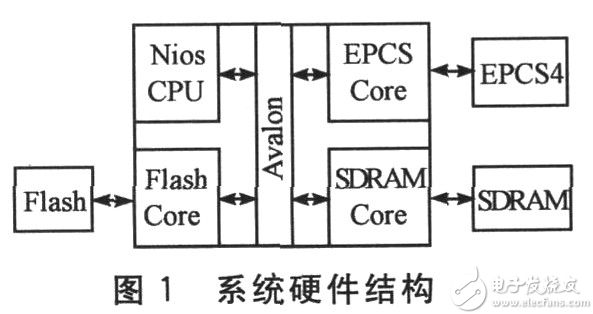
The system is mainly composed of Cyclone FPGA, EPCS, Flash and serial communication. The hardware structure is shown in Figure 1.

Click to see the original picture
EPCS uses Altera's EPCS4 with a capacity of 4 Mb, fewer pins, lower cost, and supports 3.3 V low voltage operation. The Flash chip uses AMD's Am29LV640MH/L and supports 3. OV low voltage operation, low power consumption, chip capacity of 64 Mb, for large-capacity data storage; parallel port operation, fully compatible with Cyclone FPGA, and CFI_FLASH core corresponding to SOPC, easy to design hardware circuit .
2 Working principle
2.1 Several concepts
FPGA configuration data: is a sof file, the sof file is programmed into Flash, and the FPGA can be configured from Flash after power-on. The sof file is the basis of other configuration files, and other files can be converted from the sof file.
Software data: Create an elf file through the NiosII IDE, program the user program into Flash, and allow the software program to be loaded from F1ash after resetting, thus starting the Nios II CPU.
2.2 Programming files
The programming file is a file in Flash format, ie S-reeorld ("SREC"). The SREC format is a programming format standard developed by Motorola. The SREC format file is composed of a set of ASCII codes. All hexadecimal data are in uppercase form. The structure is as follows:
1 start code. Take S as the beginning of a data line.
2 record type. A decimal number (0 to 9) that defines the type of the data field.
3 bytes. 1 byte, the number of bytes other than the address byte and check byte after the number of bytes is defined.
4 address. Consists of 4 (or 6, 8) bytes that define where the first data byte is stored.
5 data bytes. It consists of n bytes, and the data byte is the actual valid programming information.
6 check bytes. 1 byte, used for verification. All hexadecimal bytes are added and 8 bits are taken as 0xFF.
2.3 AS configuration mode
The configuration data of the FPGA is stored in the internal SRAM unit. Since the data is lost after the SRAM is powered down, the configuration data must be rewritten into the SRAM each time the power is turned on. This process is called "configuration of the FPGA." It can be seen that the configuration information of the FPGA is stored in the internal RAM of the FPGA. It can be seen that in the active serial mode, the FPGA reads the configuration data from the EPGS and stores it in the internal RAM.
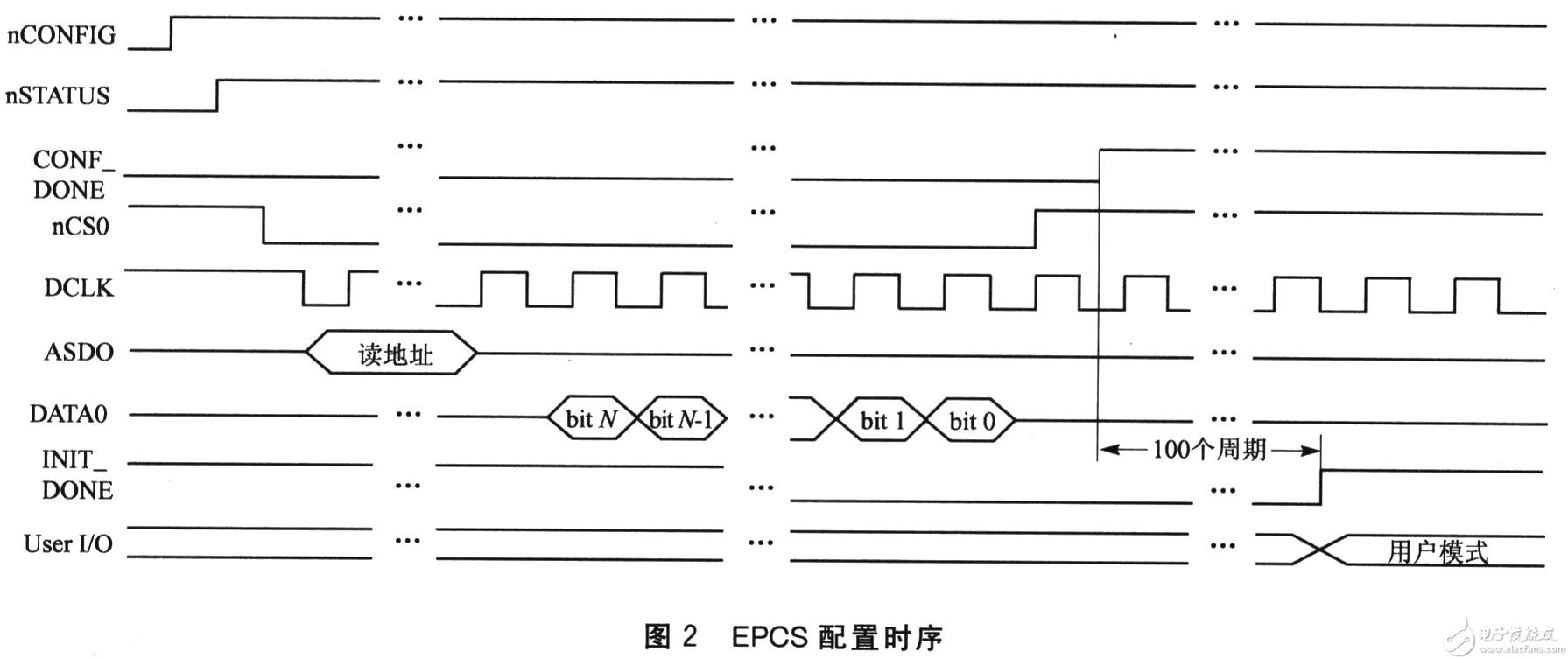
The AS configuration mode supports Stratix II and Cyclone series FPGAs. By configuring MSEL[1:O] to 1:0, the active configuration mode is selected (except for JTAG mode not controlled by MSEL, other configuration methods are determined by MSEL). The AS configuration mode uses a serial configuration device (EPCS1/EPCS4/EPCSl6/EPCS64). During the AS configuration process, the FPGAs in the StratixlI and Cy-clone families are master devices, and the serial configuration devices are slave devices. As shown in Figure 2, in the AS configuration mode, the FPGA receives configuration data via DATA0, and the configuration data and DCLK are synchronized. One bit of configuration data is transmitted every clock cycle. The configuration process is indicated by controlling nCONFIG, nSTATUS, CONF_DONE. The serial configuration chip latches the input and control signals on the rising edge of DCLK and outputs the configuration data on the falling edge. The Cyclone chip outputs a control signal on the falling edge of DCLK and latches the configuration data.

Click to see the original picture
3 Workflow
3.1 Update of hardware configuration
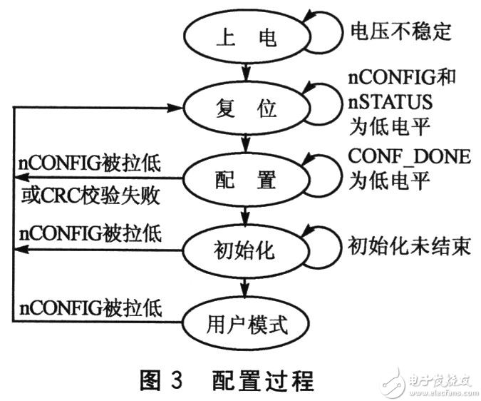
As shown in Figure 3, the FPGA configuration process is divided into: reset, configuration, and initialization.

Click to see the original picture
(1) Reset FPGA
Power-on reset: In user mode, when the nCONFIG pin is held low for 40μs, the FPGA will enter the reset state. At reset, the FP-GA samples the level of the MSEL pin to determine the configuration used; at the same time, the nSTATUS and CONF_DONE pins are asserted low by the FPGA, all I/O pins are tri-stated and the FPGA is internally configured. The register is cleared.
2 ways to reset the FPGA:
1 Add RC reset circuit or reset chip, automatically generate power-on reset pulse.
2 reference chip manual. If the chip provides a power-on reset pulse (generally a global reset signal), it is used as a reset signal; if not provided, it is found whether the chip gives the default value of the register unit power-on (usually O), and is reset by this feature. Or generate a reset pulse.
(2) Configure the FPGA
After reset, nCONFIG is pulled high by the external pull-up resistor and enters the configuration phase. At this point, nSTATUS is released by the FPGA and pulled high by the external pull-up resistor to enter the configuration state. The Cyclone chip enables the serial configuration chip by deasserting the nCSO output signal. The nCS0 pin is connected to the chip select section (nCS) of the configuration chip and is transmitted using the serial clock (DCLK) and serial data output (ASDO) pins. Operate the instructions and/or read the address signals into the serial configuration chip. The configuration chip then sends the data to the serial data output (DATA) pin, which is connected to the DATA0 input pin of the Cyclone chip. Configuration data is loaded into the FPGA on the rising edge of the DCLK clock. After receiving all configuration bits (CRC check is correct), the Cyclone chip floats the CONF_DONE pin, which is pulled high by an external 10 kΩ resistor; at the same time, the DCLK signal is stopped. Initialization begins only when CONF_DONE reaches a certain logic high level.
(3) Initialization phase
In Cyclone chips, the initial clock source is a 10MHz (typical) internal crystal of the Cyclone chip, or an optional CLKUSR pin. The internal crystal is the default initialization clock source. If an internal clock is used, the Cyclone chip provides enough clock for proper initialization. The advantage of using an internal clock is that there is no need to externally send other clocks to the CLKUSR pin during initialization, and the CLKUSR pin can be treated as an I/O pin.
(4) User mode
After the initialization is complete, the FPGA enters user mode. In user mode, the user I/O pins no longer have weak pull-up resistors, but instead perform the functions assigned in the design. The Cyclone chip can be reconfigured by pulling nCONFIG low. The nCONFIG low signal should last at least 40μs. When nCONFIG is pulled low, the Cyclone chip is reset and enters the reset phase. The Cyclone chip also pulls nSTATUS and CONF_DONE low, and all I/O pins are tri-stated. Once nCONFIG returns to logic high, the Cyclone chip will release nSTATUS and resume configuration.
(5) Errors during configuration
If an error occurs during configuration, the Cyclone chip sets the nSTA-TUS signal low to indicate a data frame error and the CONF_DONE signal is low. If the Auto-restart configuration aftererror option is selected in the General item of the Device&Pin Options window of the Quartus software, the Cyclone chip implements a reset by activating nCSO, releasing nSTATUS after the reset failure time (40μs), and attempting to configure again. If this option is not checked, the external system must monitor the nSTA-TUS signal to prevent errors and then pull the nCONFIG signal low for at least 40μs to reconfigure.
The computer establishes a connection with the Nios program on the target board, and transfers the Flash file to the FPGA through the communication interface; after the Nios program determines that the transfer file is targeted, the program data is stored in the EPCS or Flash. The received data is first temporarily stored in SDRAM instead of directly operating on EPCS and Flash. The advantage of this is that once the transfer fails or is aborted, the data in the original EPCS and Flash will not be destroyed.
When generating a Flash file by the sof2Flash command, you can open the NioslI command shell through SOPC Builder and use the "sof2 Flash-epcs-input=<input file name.sof>output=<output file name.Flash>" command to generate the Flash. The file exists in the project directory. You can also copy the sof file to "<quartus installation directory>\kits\nios2_60\examples" and open the NiosII command shell directly, using "sof2Flash-epcs-input=<input file name.sof>-output=<output file name .Flash>â€, the generated Flash file exists under “<quartus installation directory>\kits\nios2_60\examplesâ€.
Moving head beam light
Well and hight quality control
New design products
Customers design and Logo are welcomed
Quickily delivery
Competitive prices
Fit for gifts and premiums
sample can be available
OEM acceptable
Years of exporting experience as professional stage lighting manufacturer:
Senior R&D technical staff with 7 years experience in stage lighting industry;
Strict quality control in producing to maintain reliable quality;
Provide cost-effective products, wholesale price;
Professional sales team to provide perfect service.
Our company have 13 years experience of LED Display and Stage Lights , our company mainly produce Indoor Rental LED Display, Outdoor Rental LED Display, Transparent LED Display,Indoor Fixed Indoor LED Display, Outdoor Fixed LED Display, Poster LED Display , Dance LED Display ... In additional, we also produce stage lights, such as beam lights Series, moving head lights Series, LED Par Light Series and son on...
Moving Head Light Series,Beam Moving Heads Light,Beam Moving Light,Moving Head Light Beam
Guangzhou Chengwen Photoelectric Technology co.,ltd , https://www.cwledpanel.com